The Three Most Common SMT Defects and Their Cost Impact
Across the global SMT manufacturing industry, three defect types account for approximately 60–70% of all post-reflow defects: solder balls (small spherical solder particles separated from the main joint), solder bridges (unintended solder co
ections between adjacent pads or pins), and tombstones (chip components lifted on one end due to uneven wetting). Each of these defects requires manual inspection, rework, or scrap—adding $0.50–5.00 per defect in labor and material cost, and potentially $50–500 per defect if the defective product reaches the field.
The good news is that all three defect types have well-understood root causes and proven prevention strategies. This article provides a systematic root cause analysis framework and actionable process fixes for each defect, targeting a combined defect rate below 50 DPMO (defects per million opportunities)—well within IPC-A-610 Class 2 acceptance criteria.
Solder Ball Defects: Root Cause Analysis
What Are Solder Balls?
Solder balls are spherical particles of solder (typically 0.05–0.5 mm diameter) that separate from the main solder joint during reflow and deposit on the PCB surface, between component leads, or under components. They create three risks: short circuits between adjacent traces, conductive debris under BGA components that interferes with joint formation, and cosmetic defects that trigger customer rejection even when functionally benign.
Root Cause 1: Excessive Solder Paste Volume
When more solder paste is deposited than needed to form the joint, the excess paste has nowhere to go during reflow. As the paste melts and coalesces, surplus solder can separate from the main joint pool and form discrete balls. This is the most common root cause of solder balls in SMT production.
Process fix: Reduce stencil aperture area by 10–20% while maintaining the stencil thickness. For fine-pitch components (≤0.5 mm pitch), use a stepped stencil (thi
er in the fine-pitch area) or reduce aperture width to 80–90% of the pad width (home plate aperture shape for QFP/SOIC leads). Verify the reduction by measuring paste deposit volume with SPI (solder paste inspection) equipment—target 80–100% of the nominal joint volume requirement.
Root Cause 2: Solder Paste Oxidation
Solder paste that has been stored too long, exposed to humidity, or subjected to excessive temperature cycling develops oxide on the solder particle surfaces. During reflow, these oxide layers prevent the particles from coalescing smoothly—instead of merging into a single joint, some particles remain as discrete balls coated with their oxide shell.
Process fix: Enforce strict paste shelf life management (use within 6 months of manufacture, store at 2–10°C), limit paste exposure time on the stencil to ≤8 hours, and replace paste on the stencil at the start of each shift. Monitor paste condition by measuring tack strength and viscosity—paste that has lost 20% of its original tack strength is past its usable window and must be discarded.
Root Cause 3: Rapid Reflow Temperature Ramp
An overly rapid ramp through the reflow zone (>3°C/s above 200°C) causes violent flux outgassing and solder splattering. The sudden release of flux volatiles can physically propel small solder droplets away from the joint area, where they solidify as solder balls on the PCB surface.
Process fix: Limit the ramp rate above liquidus to 1.5–2.5°C/s. Ensure the time-above-liquidus (TAL) is 60–90 seconds at peak temperature 20–40°C above the solder liquidus. A gentle ramp allows flux volatiles to escape gradually rather than explosively, and gives the molten solder time to coalesce and wet the pads before the peak temperature is reached.
Root Cause 4: Inadequate Flux Activity
Flux must remove oxide from both the solder particles and the pad surface to enable coalescence. If the flux is weak (low halide content, expired, or insufficient volume relative to the solder), residual oxide prevents full particle merging, leaving solder balls behind.
Process fix: Use a solder paste with ROL1 or ROM1 flux classification per J-STD-004 for difficult-to-wet surfaces. For no-clean processes, a ROL0 flux may be sufficient if the pad surface finish is ENIG or OSP on fresh boards. Increase the flux-to-solder ratio by using a paste with higher flux content (type 3 or type 4 powder with 10–12% flux by weight).
Solder Bridge Defects: Root Cause Analysis
What Are Solder Bridges?
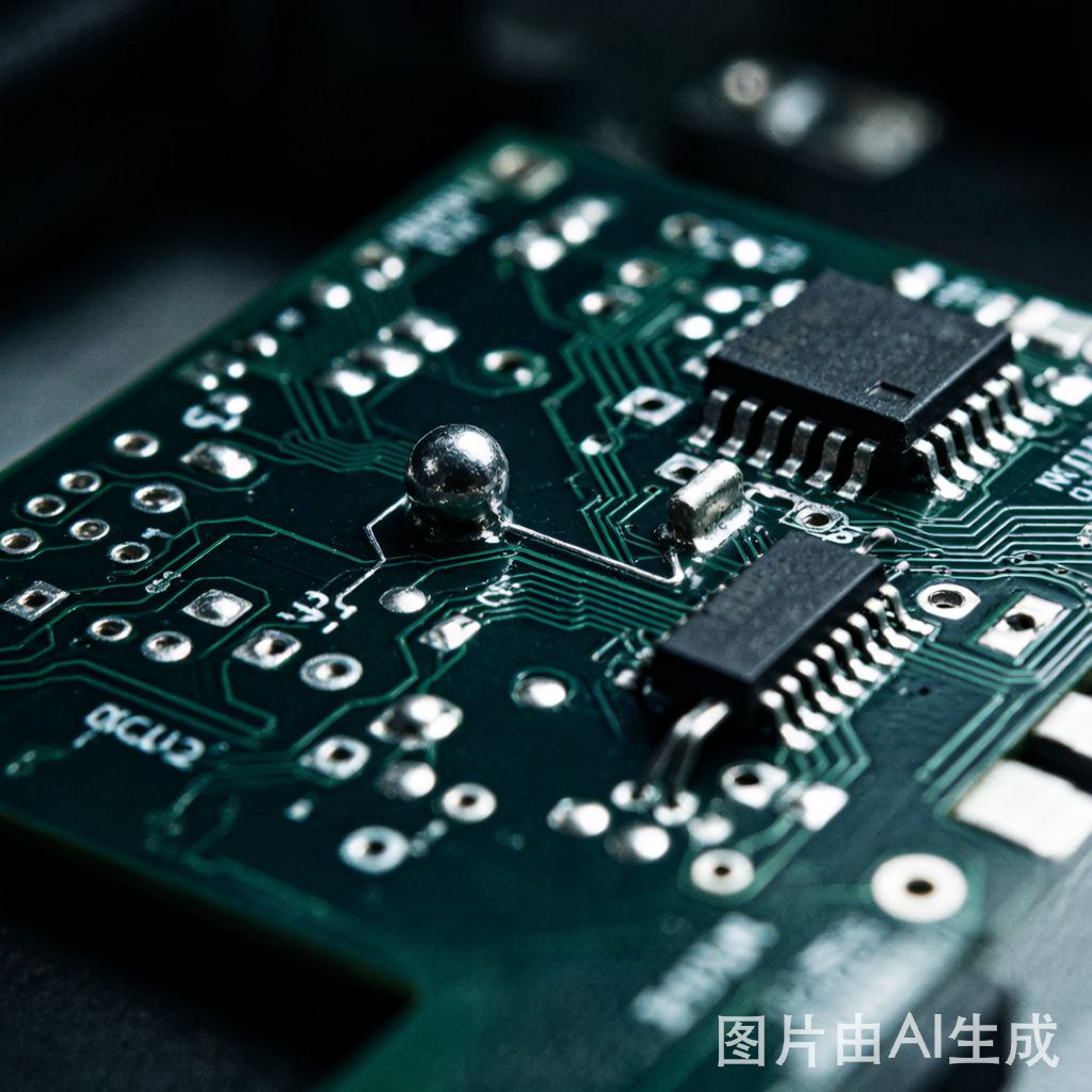
Solder bridges are unintended solder co
ections between adjacent pads or component leads. They occur most frequently on fine-pitch IC packages (QFP, QFN, BGA perimeter) where the pad-to-pad spacing is ≤0.5 mm. A bridge creates a direct electrical short circuit that must be removed by rework—typically with a soldering iron and flux, or by hot-air rework with a knife tip.
Root Cause 1: Excessive Paste Deposit Between Pads
The most common bridge mechanism is simply too much solder paste between adjacent pads. When the paste print extends beyond the pad boundary into the inter-pad gap, the excess paste melts and co
ects the two pads.
Process fix: Use aperture reduction (80–90% of pad width) for fine-pitch components, and ensure the stencil aperture is aligned precisely to the pad center (±0.025 mm alignment tolerance). For 0.4 mm pitch components, switch to a stepped stencil with 0.100 mm thickness in the fine-pitch zone (vs. 0.130 mm for standard components). This reduces the paste volume per deposit by approximately 23% in the fine-pitch area without affecting standard pitch components.
Root Cause 2: Poor Solder Paste Print Definition
If the paste print has ragged edges, smearing, or inconsistent deposit shape, the undefined paste boundaries can extend into the inter-pad gap and create bridges during reflow. Poor print definition is caused by worn stencil apertures, inappropriate squeegee pressure, or paste with insufficient viscosity.
Process fix: Inspect stencil apertures weekly for wear and smearing—replace the stencil when aperture edges show rounding or burring. Optimize squeegee pressure (typically 3–6 kg for a 250 mm blade) and speed (20–50 mm/s) to achieve clean paste release. Use a paste with appropriate viscosity for the stencil design (type 3 powder for 0.130 mm stencil, type 4 or 5 for 0.100 mm stepped stencil). Monitor print quality with SPI—reject any deposit that extends beyond the pad boundary by more than 25% of the inter-pad gap.
Root Cause 3: Solder Wetting onto Adjacent Traces
Solder can bridge between pads by wetting along co
ected copper traces that route between the pads. If a trace passes through the gap between two fine-pitch pads, the solder can wet the trace surface and create a continuous solder path from one pad to the other.
Process fix: In the PCB design, avoid routing traces between fine-pitch pads (≤0.5 mm pitch). If routing between pads is unavoidable, ensure the trace width is ≤50% of the inter-pad gap and the solder mask completely covers the trace in the inter-pad gap area. Specify solder mask dams between all fine-pitch pads—these are narrow (0.05–0.10 mm) solder mask strips that physically prevent solder from spreading between adjacent pads.
Root Cause 4: Component Misalignment
If a component shifts during reflow so that its leads overlap adjacent pads, the solder that was intended for two separate pads merges into a single bridge co
ecting the overlapping lead to both pads.
Process fix: Verify placement accuracy with post-placement AOI—target ±0.05 mm for fine-pitch components. Ensure the placement force is adequate to embed component leads 50–70% into the paste deposit, providing adhesion that resists surface-tension-driven shift during reflow. For QFN and QFP packages, increase the pad-to-lead width ratio (pad width 1.5× lead width) to provide a larger wetting target that tolerates minor misalignment.
Tombstone Defects: Root Cause Analysis
What Are Tombstones?
Tombstones (also called drawbridging or Manhattan effect) occur when a chip component (0402, 0603, 0805) lifts on one end during reflow, standing upright like a tombstone. The root mechanism is always unequal wetting: one end of the component wets to its pad first, and the surface tension of the wetted joint pulls the component upward before the other end has wetted. The result is a component with one end soldered to its pad and the other end standing free—an open circuit.
Root Cause 1: Unequal Pad Size or Thermal Mass
If the two pads for a chip component have different sizes or are co
ected to different copper pour areas, they reach reflow temperature at different times. The pad with less thermal mass (smaller pad, less copper co
ection) reaches liquidus first and wets the component lead, pulling it upward before the other pad has melted its paste.
Process fix: Design chip component pads with identical dimensions per IPC-7351. Ensure both pads have identical copper pour co
ections—if one pad co
ects to a large ground plane, add thermal relief spokes (2 or 4 spokes, 0.25 mm width) to equalize the thermal mass. For components on heavy copper (2 oz or 3 oz), thermal relief on both pads is mandatory to prevent tombstoning.
Root Cause 2: Unequal Solder Paste Volume
If one pad receives more paste than the other, the pad with more paste has a larger molten solder volume that exerts more surface tension force. The stronger force pulls the component toward that pad, lifting the opposite end.
Process fix: Use SPI to verify that paste deposit volumes on paired pads are within ±15% of each other. If variation exceeds this threshold, investigate stencil aperture alignment and squeegee pressure consistency. For 0402 components, switch to type 4 or type 5 solder paste powder (20–25 μm and 10–15 μm particle sizes respectively) to improve print consistency on the small apertures required for these components.
Root Cause 3: Uneven Reflow Profile
Temperature gradients across the reflow oven (zone-to-zone or left-to-right) can cause one side of the board to reach liquidus before the other. Components near the hotter side of the board wet first, creating a systematic tombstone pattern concentrated on one side of the assembly.
Process fix: Profile the reflow oven with a 12-point thermocouple board per IPC-7530, measuring temperature at both the left and right edges and at multiple positions along the conveyor direction. Adjust zone temperatures and conveyor speed to achieve ±5°C uniformity across the board width at the peak zone. If the oven has a cross-zone gradient that ca
ot be eliminated, reduce the ramp rate through the reflow zone to give both sides of the board more time to reach equilibrium temperature.
Root Cause 4: Component Placement Offset
If a chip component is placed off-center so that one end is closer to its pad center and the other end is near the pad edge, the centered end has better paste contact and wets faster. The offset end has less paste contact area, delays wetting, and lifts.
Process fix: Set placement tolerance to ±0.05 mm for 0402/0603 components. Verify placement accuracy with post-placement AOI. If the pick-and-place machine ca
ot achieve this accuracy consistently on small components, check nozzle condition (worn tips cause centering errors) and vision calibration.
Systematic Defect Prevention Framework
Instead of chasing individual defects reactively, implement a systematic framework that prevents all three defect types simultaneously:
- Stencil design review: Before production, verify that stencil apertures provide 80–100% of the required joint volume for each component type. Use stepped stencils for mixed-pitch boards. Verify aperture alignment to pad centers.
- SPI monitoring: Implement SPI (solder paste inspection) on 100% of paste deposits for fine-pitch and chip components. Set volume tolerance to ±20% for standard components and ±15% for chip components and fine-pitch ICs.
- Reflow profile optimization: Profile the oven with a multi-point thermocouple board every shift. Verify ramp rate ≤2.5°C/s above liquidus, TAL 60–90s, peak temperature within ±5°C across the board width.
- Paste management discipline: Enforce paste shelf life, stencil exposure time limits (≤8 hours), and paste replacement at each shift start. Monitor paste tack and viscosity weekly.
- Post-reflow AOI: Implement 100% AOI inspection for solder balls (visual detection), bridges (electrical + visual), and tombstones (visual detection). Feed AOI data back to the process engineers for root cause analysis and continuous improvement.
With this framework in place, the combined solder ball + bridge + tombstone defect rate should drop below 50 DPMO within 4–6 weeks of implementation—well within the quality targets for most SMT production operations.
Conclusion
Solder balls, solder bridges, and tombstones are the three most common SMT assembly defects, but they are also the most preventable. Each has clear root causes in stencil design, paste management, reflow profiling, and component placement—and each has equally clear process fixes that eliminate the root cause. The key is moving from reactive rework to proactive prevention: validate stencil design before production, monitor paste deposits with SPI, profile the reflow oven regularly, and use AOI data for continuous improvement. When these practices are implemented systematically, defect rates drop below 50 DPMO and rework costs decrease by 80–90%—transforming defect prevention from a cost center into a competitive advantage.