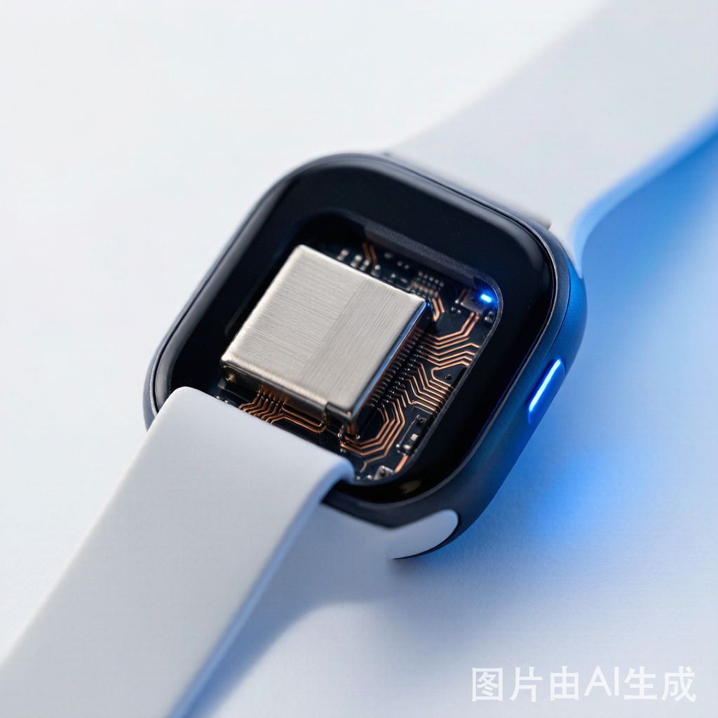
## The EMI Challenge in IoT and Wearable Devices
IoT and wearable electronics face unique electromagnetic interference challenges that traditional shielding approaches ca
ot adequately address. These compact devices operate in crowded RF environments—2.4GHz WiFi, Bluetooth, Zigbee, and emerging 5G NR signals all compete for spectrum space while the device itself generates internal noise from high-speed digital clocks, switching power supplies, and RF transmitters.
The miniature form factor of wearables (typically 30-50mm × 30-50mm PCB area) means that ante
a elements, digital circuits, and power management sit within millimeters of each other. Without effective RF shielding, self-interference can degrade receiver sensitivity by 10-15dB, reduce battery life through increased retransmissions, and cause regulatory compliance failures for emissions standards like FCC Part 15 and ETSI EN 300 328.
## Why Nickel-Plated Brass for IoT Shielding
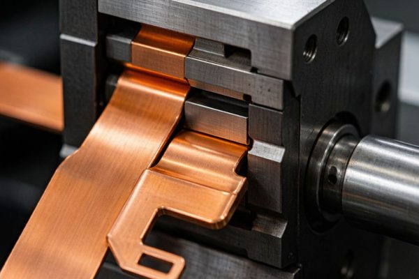
Nickel-plated brass has emerged as the optimal shielding material for compact IoT and wearable devices, offering a combination that pure copper or stainless steel ca
ot match:
### Material Properties Comparison
| Property | Nickel-Plated Brass | Pure Copper | Stainless Steel 304 |
|———-|——————-|————-|———————|
| Shielding effectiveness (1GHz) | 85-95 dB | 90-100 dB | 70-80 dB |
| Shielding effectiveness (5GHz) | 70-80 dB | 75-85 dB | 55-65 dB |
| Formability (deep draw) | Excellent | Good | Poor |
| Solderability | Good (nickel barrier) | Excellent | Poor |
| Corrosion resistance | Excellent | Poor (oxidizes) | Excellent |
| Density | 8.5 g/cm³ | 8.9 g/cm³ | 7.9 g/cm³ |
| Cost per unit area | Moderate | Moderate | Low |
The nickel plating on brass provides three critical advantages for IoT devices:
1. Corrosion protection: Nickel prevents brass tarnishing in humid Southeast Asian climates, maintaining shielding effectiveness over the device lifetime
2. Solderability barrier: Nickel acts as a diffusion barrier, preventing zinc from brass migrating into solder joints during SMT assembly
3. Surface hardness: Nickel (typically 3-5μm electrolytic or 5-8μm electroless) provides scratch resistance during automated assembly handling
## Shield Geometry Optimization for Miniature Devices
### Fence-and-Cover Architecture
The traditional fence-and-cover approach adapts well to IoT devices when properly miniaturized:
– Fence height: 2.0-3.0mm (sufficient for most IoT RF isolation needs)
– Fence wall thickness: 0.15-0.25mm nickel-plated brass
– Cover thickness: 0.1-0.15mm nickel-plated brass
– Fence-to-cover engagement: Snap-fit tabs or solder-down clips at 3-5mm intervals
Design tip: For wearable devices, reduce fence height to 1.5mm by placing the shield directly over the RF transceiver chip and its immediate support circuits. This localized shielding approach saves 40% volume compared to full-module shielding.
### Perimeter Frame Shield
A perimeter frame shield surrounds the sensitive circuit area without a top cover, relying on ground plane isolation for vertical shielding:
– Frame width: 1.0-1.5mm nickel-plated brass strip, formed into rectangular frame
– Ground via fence: Row of ground vias at 1.0mm spacing along the i
er frame edge
– Application: Best for devices where vertical EMI coupling is naturally suppressed by PCB ground plane design
– Volume savings: 60-70% compared to full fence-and-cover
### Multi-Cavity Shield
For IoT devices with multiple isolated RF sections (e.g., separate Bluetooth and WiFi modules), multi-cavity shields divide the shielded area into separate compartments:
– Internal walls: 0.15mm nickel-plated brass dividers soldered to PCB ground
– Cavity isolation: 40-50dB between adjacent compartments at 2.4GHz
– Manufacturing: Progressive die stamping produces multi-cavity shields in single operation
## Miniaturization Strategies Below 5mm Form Factor
When wearable device PCBs shrink below 5mm width, traditional shield cans become impractical. Alternative strategies include:
### Shield-in-Package (SiP) Approach
Integrate shielding directly into the IC package by applying conformal nickel-plated brass foil over the die:
– Foil thickness: 0.05mm electroless nickel-plated brass
– Application: Die-level shielding before SMT placement
– Isolation: 30-40dB at 2.4GHz from adjacent packages
– Advantage: No PCB-level shield needed, maximum space efficiency
### Board-Level Copper Pour Isolation
Use heavy copper pour (2oz or 3oz) with via fences to create ground-isolated zones:
– Ground pour width: 2.0mm minimum around sensitive circuits
– Via fence: Via-in-pitch at 0.8mm spacing, 0.3mm via diameter
– Isolation: 20-30dB at 2.4GHz (less than metal shield but often sufficient for wearable RX sensitivity)
### Conductive Coating Shielding
Apply conductive nickel-based paint or silver-filled epoxy to the device housing interior:
– Coating thickness: 25-50μm dry film
– Shielding effectiveness: 30-50dB at 1-6GHz
– Application: Post-assembly coating on plastic wearables where internal metal shields are impractical
## SMT Assembly Considerations
Nickel-plated brass shields introduce specific SMT assembly requirements:
### Reflow Soldering Compatibility
– Peak temperature: 260°C maximum (nickel plating integrity maintained)
– Time above liquidus: 60-90 seconds (SAC305 compatible)
– Thermal profile: Shields act as heat sinks—increase zone temperatures by 5-10°C near shielded areas
– Void control: Nickel surfaces require active flux for reliable solder wetting
### Pick-and-Place Handling
– Shield weight: Typical IoT shield 0.5-2.0g—requires nozzle with 3-5mm tip diameter
– Placement accuracy: ±0.1mm for fence-to-PAD alignment
– Tape packaging: Shields ship in embossed tape (8mm or 12mm width) with protective film over snap-fit features
### Rework Procedures
– Shield removal: Hot air tool at 300°C with shield-specific nozzle
– Replacement: New shield required after removal (snap-fit tabs fatigue after one cycle)
– Inspection: X-ray verification of solder joint integrity under fence walls (AOI ca
ot see under the shield)
## Regulatory Compliance and Testing
IoT devices require EMI compliance testing with shields installed:
### FCC Part 15 (US Market)
– Radiated emissions: Shield must reduce emissions below limits at 30MHz-6GHz
– Conducted emissions: Shield grounding must provide <5mΩ contact resistance to PCB ground
– Test configuration: Measure with shield installed, then compare baseline without shield
### ETSI EN 300 328 (European Market)
– Spurious emissions: Shield effectiveness validated across 2.4GHz band
– Receiver sensitivity: Shield must not degrade ante
a performance (verify ante
a pattern with shield present)
### Southeast Asian Markets
– Thailand TIS: Follow ETSI requirements with additional humidity testing
– Vietnam QCVN: Apply FCC-style limits with local certification process
– Malaysia MCMC: Combined FCC/ETSI approach
## Conclusion
Nickel-plated brass RF shielding provides the optimal balance of electromagnetic performance, mechanical formability, and manufacturing compatibility for IoT and wearable electronics. By selecting appropriate shield geometry—fence-and-cover, perimeter frame, or multi-cavity designs—engineers can achieve 70-95dB shielding effectiveness within the tight volume constraints of compact devices. TechMartSE supplies precision nickel-plated brass strips and pre-formed shield components tailored for IoT device manufacturing, with thickness options from 0.1mm to 0.3mm and nickel plating specifications meeting SMT assembly requirements.