## What Is First Article Inspection in SMT Manufacturing?
First Article Inspection (FAI) is the systematic verification process performed on the first production sample of any new SMT assembly, component, or process change. It confirms that the manufacturing setup, materials, and processes produce parts that meet all design specifications before full production release.
For copper component validation specifically, FAI ensures that copper strips, brass contacts, nickel-plated shielding cans, and other metallic SMT components conform to dimensional, material, and functional requirements. This inspection follows established frameworks—AS9102 for aerospace applications, IPC-6012 for PCB fabrication, and IPC-A-610 for solder joint acceptability.
In Southeast Asian SMT manufacturing, where production volumes are high and defect costs escalate rapidly, FAI serves as the critical gate between prototype qualification and volume production. A thorough FAI on copper components typically prevents 80-90% of production escapes that would otherwise require costly rework or field returns.
## FAI Framework: AS9102 Three-Form Structure
While AS9102 was developed for aerospace, its three-form structure provides an excellent framework for any SMT copper component FAI:
### Form 1: Part Number Accountability
Document every characteristic that must be verified:
– Part identification: Drawing number, revision, part number, serial number of first article
– Characteristic numbering: Assign unique numbers to every dimension, material property, and functional requirement from the engineering drawing
– Source documentation: Reference drawing callouts, specification paragraphs, and customer requirements for each characteristic
– Copper component specifics: Include material certification (alloy, temper, grain size), plating specification (type, thickness), and dimensional tolerances
### Form 2: Product Verification
Record actual measurement results against requirements:
– Dimensional measurements: Every dimension with tolerance—length, width, thickness, hole diameter, bend angle
– Material verification: Alloy composition per mill cert, mechanical properties (yield, tensile, elongation), plating thickness per XRF measurement
– Visual inspection: Surface condition, plating coverage, stamping defect absence
– Characteristic-by-characteristic: Each numbered characteristic gets a pass/fail determination with actual measured value
### Form 3: Process Verification
Confirm that production processes are capable:
– Tool verification: Die/stamping tool certification, press to
age calibration
– Process parameters: Stamping speed, a
ealing temperature profile, plating bath composition
– Equipment calibration: Measurement tool calibration records (CMM, XRF, optical comparator)
– Special processes: Solderability testing per J-STD-002 if component requires soldering
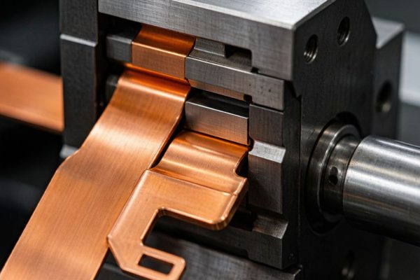
## Copper Component Dimensional Validation
### Thickness Measurement
Copper strip thickness is the most critical dimension for SMT components:
– Measurement tool: Digital micrometer (0.001mm resolution) for strip; CMM for formed parts
– Sampling plan: Measure at 5 locations across strip width (center, quarter-points, edges)
– Acceptance: ±0.005mm for strips ≤0.3mm; ±0.01mm for strips >0.3mm
– Special consideration: Thickness variation across width indicates rolling misalignment—reject if >50% of tolerance band consumed
### Width and Length Measurement
– Strip width: Optical comparator or laser micrometer, ±0.01mm tolerance typical
– Formed part length: CMM measurement with GD&T evaluation if position tolerances apply
– Bend angle: Protractor measurement or CMM angular evaluation, ±0.5° typical for SMT contact bends
### Hole and Slot Features
– Hole diameter: Pin gauge set for through-holes, optical measurement for micro-holes <0.5mm
– Slot width: Optical comparator with digital readout
– Position accuracy: CMM measurement relative to datum features, positional tolerance per drawing callout
## Material Certification Verification
### Mill Test Certificate Review
Every copper component FAI must include mill test certificate (MTC) verification:
– Alloy verification: Chemical composition matches specification (C11000 = 99.9% Cu, C26000 = 70% Cu/30% Zn)
– Mechanical properties: Yield strength, tensile strength, and elongation per specification temper
– Grain size: Stated grain size number per ASTM E112 (critical for formed components)
– Plating certification: Nickel thickness (μm), gold thickness if applicable, porosity test results
### Independent Material Verification
Beyond MTC review, FAI should include independent verification:
– XRF analysis: Confirm alloy composition at 3 locations on the component
– Hardness test: Micro-Vickers hardness (HV0.1) for temper verification
– Plating thickness: XRF cross-sectional measurement at 5 locations
– Cross-section metallography: Verify grain structure and plating adhesion for critical components
## Electrical Testing for Copper SMT Components
### Contact Resistance Measurement
For copper contacts and co
ector components:
– Test method: Four-wire Kelvin measurement per EIA-364-23
– Acceptance criteria: Contact resistance ≤5mΩ for power contacts, ≤20mΩ for signal contacts
– Environment: Measure at room temperature (23°C ±2°C) after 10 mating cycles
– Special test: Low-level contact resistance (LLCR) per EIA-364-23 for tin-plated contacts (10mV, 100mA test current to avoid fritting)
### Current Carrying Verification
For copper bus bars and power distribution components:
– Test current: Rated current ×1.25 for 1-hour thermal stability test
– Temperature rise: Measure ΔT at 5 points on the component, maximum ΔT ≤30°C above ambient
– Voltage drop: Measure at rated current, verify against specification limit
– Thermal imaging: IR camera scan during current test identifies hot spots from cross-section variation
### Solderability Testing
All copper SMT components requiring solder attachment must pass solderability validation:
– J-STD-002 Category 3: Most stringent—wetting <2 seconds after 8-hour steam aging (95°C, 85% RH)
– Test method: Dip-and-look in 235°C SAC305 solder pot with active flux
– Acceptance: ≥95% wetting coverage on all solderable surfaces
– Frequency: Every lot change requires solderability re-validation
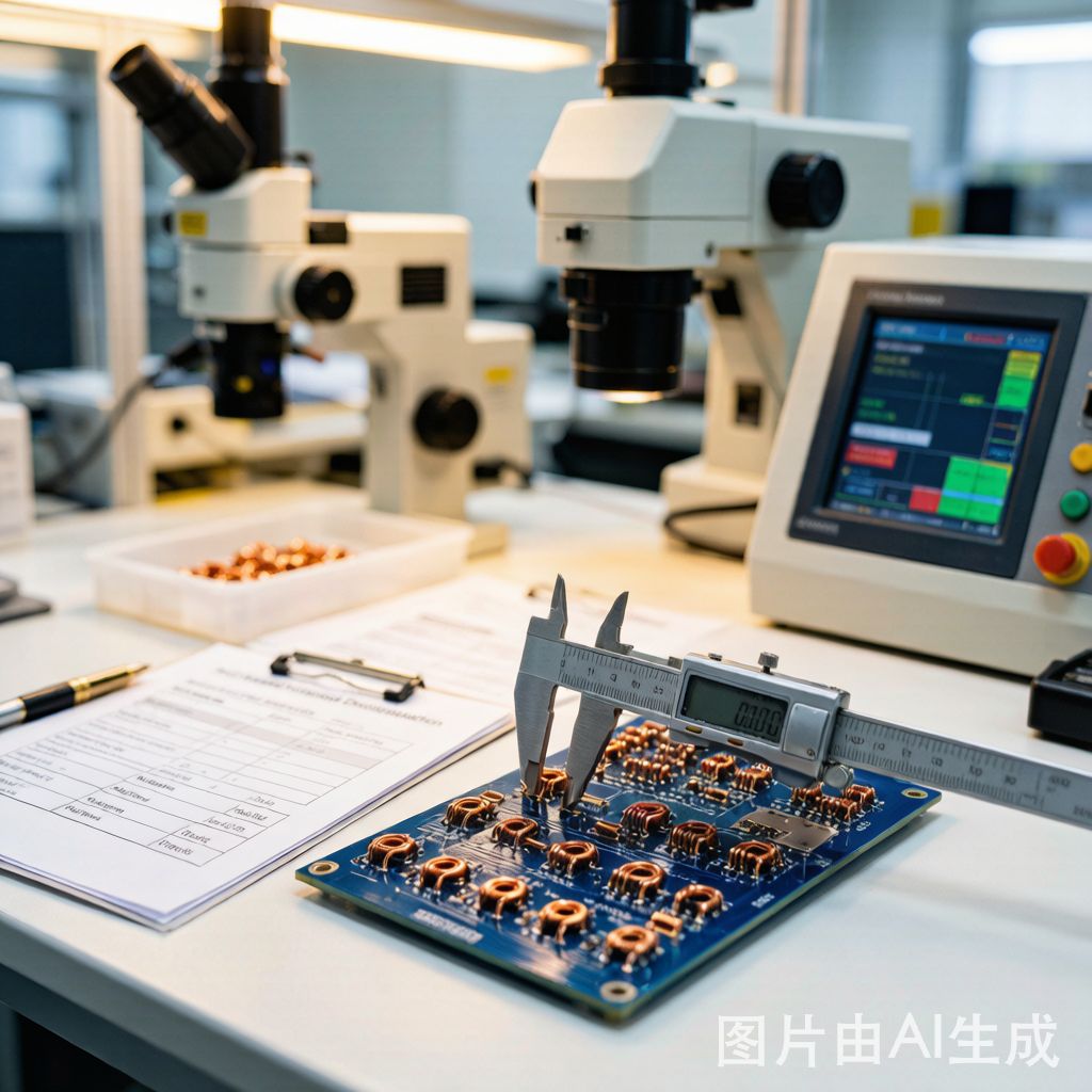
## FAI Documentation and Approval Process
### Documentation Package Contents
A complete SMT copper component FAI package includes:
1. FAI forms: Completed AS9102 Forms 1, 2, 3 (or equivalent company-specific forms)
2. Dimensional report: All measurements with tolerance comparison
3. Material certifications: Mill test certificates, independent XRF and hardness data
4. Plating reports: Thickness measurements, porosity tests, adhesion tests
5. Electrical test data: Contact resistance, current carrying, solderability results
6. Photographs: Macro photos of critical features, defect-free verification
7. Process records: Stamping parameters, a
ealing profiles, plating bath logs
8. Calibration records: All measurement equipment calibration certificates
### Approval Workflow
– FAI engineer: Compiles data, makes characteristic-by-characteristic pass/fail determination
– Quality manager: Reviews FAI package, approves or rejects with disposition
– Customer approval: Required for customer-specific parts—submit package for customer FAI review
– Production release: Only after full FAI approval—no production without FAI sign-off
## Common FAI Failures for Copper Components
Understanding typical failure modes helps focus inspection effort:
1. Thickness out-of-tolerance: Rolling variation across strip width (most common failure)
2. Grain size too coarse: Over-a
ealed material showing G4-G5 (orange peel risk)
3. Plating thickness non-conformance: Nickel plating thin at edges, thick at centers
4. Bend angle deviation: Spring-back exceeding prediction after forming
5. Solderability failure: Oxidation during storage or transport reducing wetting
6. Dimensional shift: Progressive die wear causing feature drift over production run
## Conclusion
SMT First Article Inspection for copper components is the essential gateway between design qualification and volume production. By systematically verifying dimensional accuracy, material certification, plating integrity, and electrical performance per AS9102 and IPC frameworks, manufacturers prevent production escapes and ensure consistent quality. TechMartSE supports FAI processes by providing complete mill test certificates, grain size data, and plating specifications with every copper strip and brass component shipment, enabling Southeast Asian SMT manufacturers to execute thorough first article validation efficiently.