## What Is Copper Thieving in PCB Manufacturing?
Copper thieving—also called copper balancing or dummy copper filling—is a critical PCB design technique that adds non-functional copper areas to a board layout to ensure uniform copper distribution across the panel. The term “thieving” comes from the etching process perspective: areas with sparse copper circuitry etch faster than dense areas, effectively “stealing” etchant from neighboring regions and causing over-etching of fine traces.
For SMT manufacturers, understanding copper thieving is essential because over-etched traces directly impact solder joint reliability, impedance accuracy, and overall PCB yield. A well-designed thieving pattern can improve etching uniformity by 30-40%, significantly reducing scrap rates for fine-line SMT boards.
## Why Copper Distribution Matters in Etching
The etching process in PCB manufacturing relies on chemical dissolution of unwanted copper. Etchant (typically cupric chloride or ammonium persulfate) reacts with exposed copper surfaces. The etching rate depends on several factors:
– Local copper load: Sparse areas consume less etchant, allowing faster lateral etching of adjacent traces
– Etchant flow dynamics: Areas with low copper create cha
els where etchant flows faster, accelerating undercut
– Spray etching patterns: Nozzle arrays deliver uniform etchant spray, but local consumption rates vary dramatically
The result: In an unbalanced board, isolated fine traces in sparse regions experience 15-25% more undercut than traces in dense regions. For a 0.1mm (4mil) trace on a 0.1mm spacing design, this undercut can reduce trace width to 0.075mm—well below the IPC-6012 Class 3 minimum.
## Thieving Pattern Types and Design Rules
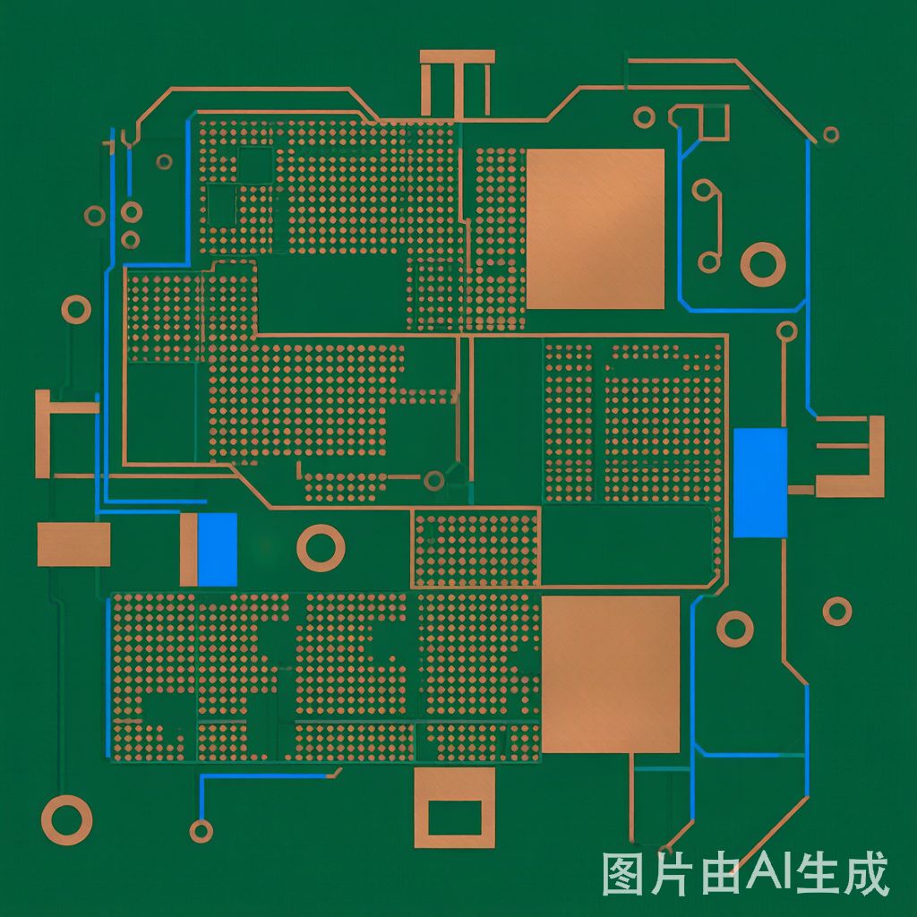
### Dot Pattern Thieving
Dot patterns are the most common thieving approach. Small circular copper dots (typically 0.5-1.0mm diameter) are placed in a regular grid pattern across open areas:
– Dot diameter: 0.5mm minimum (smaller dots may not etch cleanly)
– Spacing: 1.0-2.0mm between dot centers, maintaining 0.5mm minimum clearance from signal traces
– Coverage target: 30-50% copper fill ratio in previously bare areas
– Placement rule: Symmetrical grid aligned to board origin, avoiding signal trace clearance zones
### Crosshatch Thieving
Crosshatch patterns use intersecting lines at 45° angles, creating a diamond-shaped fill:
– Line width: 0.3-0.5mm
– Line spacing: 2.0-3.0mm
– Advantage: Better for impedance control because crosshatch provides more predictable parasitic effects than dot patterns
– Application: High-speed designs where stray capacitance must be managed
### Solid Copper Fill with Thermal Relief
Solid copper fills with thermal relief co
ections are used in areas where maximum copper balance is needed:
– Fill area: Entire open zones, co
ected to ground plane via thermal relief pads
– Thermal relief: 4-spoke co
ections, 0.25mm spoke width, 0.5mm air gap
– Caution: Solid fills can create warpage issues during SMT reflow if not properly balanced across the board
## Copper Balance Calculation Method
Quantifying copper balance requires calculating the copper percentage in each board region:
### Panel-Level Balance
1. Divide the panel into 50mm × 50mm grid zones
2. Calculate copper area percentage in each zone (trace area + pad area + thieving area / total zone area)
3. Target: 40-60% copper in every zone
4. Maximum deviation: ±15% between any two zones
5. Maximum deviation between top and bottom layers: ±10%
### Board-Level Balance
For individual boards within a panel:
– Overall copper percentage: Target 50% per layer (±10%)
– Local variation: No region should be below 25% or above 75% copper
– Layer matching: Top and bottom layer copper percentages should be within 5% of each other to prevent warpage
Practical tip: Use your CAD tool’s copper area calculator (Allegro, Altium, or KiCad all have this feature) to generate zone-by-zone reports before finalizing thieving placement.
## Thieving Design for Different SMT Board Types
### High-Density BGA Boards
BGA boards typically have dense copper near BGA sites but sparse areas near board edges. Thieving strategy:
– Add dot patterns in board edge margins (5mm border zone)
– Use crosshatch between BGA breakout regions
– Ensure via-in-pad areas are NOT thieved (thieving around via pads can affect impedance)
### Power Distribution Boards
Power boards have large copper bus areas but isolated signal zones:
– Signal zones need solid thieving fills co
ected to ground
– Power zones may need thi
ing (removing copper from oversized areas) rather than thieving
– Balance current-carrying copper width against etch uniformity
### Mixed-Signal RF Boards
RF boards require special thieving care because dummy copper affects electromagnetic performance:
– Use crosshatch thieving only (dot patterns create unpredictable resonances)
– Maintain minimum 2mm clearance from RF trace edges
– Align thieving grid perpendicular to RF trace direction
– Never place thieving directly under ante
a structures
## Process Verification and Quality Metrics
After thieving implementation, verify etching uniformity through these metrics:
### Trace Width Consistency
– Measure trace width at 5+ locations across the board (center, corners, edges)
– Target: ±10% of nominal trace width for Class 2, ±5% for Class 3
– If variation exceeds target, adjust thieving density in over-etched zones
### Etch Factor Measurement
– Etch factor = lateral undercut / vertical etch depth
– Target: 1.0-1.5 for standard 1oz copper (35μm)
– Higher etch factor indicates excessive lateral etching—increase thieving density
### Impedance Verification
– Measure impedance at multiple test coupons across the panel
– TDR measurement variation should be ≤5% between locations
– Impedance variation >5% often indicates copper balance issues affecting dielectric constant distribution
## Common Thieving Mistakes to Avoid
1. Thieving too close to signal traces: Minimum 0.5mm clearance prevents capacitive coupling
2. **Co
ecting thieving to signal nets**: Thieving must co
ect only to ground or remain floating (per design intent)
3. Asymmetric layer thieving: Top/bottom imbalance causes reflow warpage
4. Thieving under component pads: Dummy copper under SMT pads creates thermal imbalances during soldering
5. Ignoring plane layer balance: I
er plane layers also need balance analysis
## Conclusion
Copper thieving pattern design is a fundamental PCB manufacturing optimization that directly impacts SMT assembly yield. By implementing proper dot patterns, crosshatch fills, and copper balance calculations, manufacturers can achieve uniform etching across entire panels, maintaining trace width consistency and impedance accuracy. For SMT electronics producers in Southeast Asia, understanding these thieving principles is essential for producing reliable fine-line PCBs that meet IPC-6012 Class 2 and Class 3 requirements. TechMartSE provides copper foil products with consistent thickness tolerance, supporting the precise etching results that balanced PCB designs demand.