Why Tropical Environments Accelerate Copper Trace Degradation
Southeast Asia presents some of the most challenging environmental conditions for electronic hardware. Average a
ual humidity ranges from 70–90% RH across Thailand, Vietnam, Malaysia, Indonesia, and the Philippines. Coastal industrial zones add salt mist exposure, and operating temperatures routinely exceed 40°C in factory and outdoor installations. Under these conditions, copper PCB traces—normally protected by solder mask and surface finish—face two insidious degradation mechanisms: corrosion (chemical oxidation of copper) and electromigration (voltage-driven metal ion transport that forms conductive dendrites between traces).
Both mechanisms are dramatically accelerated by moisture. A PCB operating at 85°C/85% RH experiences 10–50× faster corrosion and electromigration growth than the same board at 25°C/40% RH. For electronics manufacturers targeting the Southeast Asian market, understanding and mitigating these failure modes is not optional—it is a product survival requirement.
Copper Corrosion Mechanisms in Humid Environments
Atmospheric Corrosion of Bare Copper
When copper is exposed to humid air containing oxygen and trace contaminants, it forms a sequence of corrosion products:
- Cu₂O (cuprous oxide): Forms first as a thin (10–50 nm) reddish-brown layer. This layer is semi-protective—it slows further oxidation but does not completely seal the surface.
- CuO (cupric oxide): Develops on top of Cu₂O at elevated temperatures (>100°C) or in the presence of strong oxidizers. Black and non-protective, it allows continued copper dissolution.
- Cu₂(OH)₂CO₃ (basic copper carbonate, patina): The green coating commonly seen on exposed copper in outdoor environments. Formed by reaction with atmospheric CO₂ and moisture. This layer provides moderate protection but is porous and can delaminate under thermal cycling.
- Cu₂S / CuS (copper sulfide): Forms in environments containing H₂S or SO₂ (common near industrial zones and volcanic areas in Indonesia and Thailand). Copper sulfide is electrically semi-conductive, creating leakage paths between adjacent traces.
The corrosion rate of bare copper at 85% RH, 40°C, with 0.1 ppm SO₂ is approximately 0.5–1.0 μm/year. At 95% RH with 1 ppm SO₂ (typical of coastal industrial areas), the rate increases to 3–5 μm/year—enough to consume a 35 μm (1 oz) copper trace in 7–12 years.
Solder Mask as a Corrosion Barrier
LPI (liquid photoimageable) solder mask is the primary barrier protecting copper traces from atmospheric corrosion. However, solder mask is not impermeable—it has a moisture absorption rate of 0.5–1.5% by weight at 85% RH, and it contains microscopic pinholes and edge coverage defects that allow moisture to reach the copper surface. Key solder mask vulnerabilities in tropical environments:
- Edge coverage on narrow traces: Solder mask over 0.1 mm (4 mil) traces may have only 50–70% edge coverage, leaving the trace sidewalls partially exposed. In humid environments, corrosion initiates at these exposed sidewalls and propagates under the mask.
- Pinhole defects: Solder mask typically contains 1–5 pinholes per cm², each providing a direct moisture path to the copper surface. Pinholes are particularly problematic near via holes and component pads where mask registration is most difficult.
- Thermal cycling delamination: Repeated thermal cycling (day/night temperature swings of 15–25°C in tropical outdoor installations) causes differential expansion between the solder mask and copper, leading to micro-cracking and delamination at the mask-copper interface.
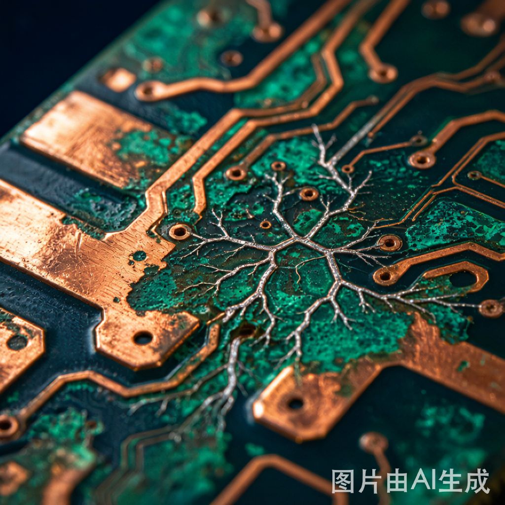
Electromigration: Voltage-Driven Dendrite Growth
The Electromigration Mechanism
Electromigration on PCBs is a voltage-driven process in which metal ions dissolve from one trace (the anode), migrate through a moisture film on the PCB surface, and deposit on an adjacent trace (the cathode), forming a conductive dendrite. The dendrite grows progressively from the cathode toward the anode, and when it bridges the gap, it creates a short circuit that can cause catastrophic failure.
The electromigration rate follows an exponential relationship with humidity: below 60% RH, dendrite growth is negligible (months to years for bridging). Above 75% RH, the moisture film on the PCB surface provides sufficient ionic conductivity for rapid dendrite growth—bridging times of hours to days for typical PCB trace spacings. At 85% RH, with 5V bias between adjacent 0.15 mm-spaced traces, copper dendrites can bridge the gap in 48–200 hours depending on surface contamination.
Contamination Acceleration
Surface contamination dramatically accelerates electromigration by providing ionic species that increase the conductivity of the moisture film:
- Flux residues: No-clean flux residues contain organic acids (abietic acid, carboxylic acids) that dissociate in water to provide highly mobile ions. Boards processed with no-clean flux exhibit 5–10× faster dendrite growth than water-cleaned boards at the same humidity.
- Hand contamination: Sodium chloride from fingerprints (human sweat contains 0.9% NaCl) is one of the most aggressive electromigration accelerators. A single fingerprint between two biased traces can reduce the bridging time from weeks to hours.
- Process chemical residues: Etching solution residues (FeCl₃, CuCl₂), cleaning solvent residues, and even dust from cardboard packaging can provide ionic contamination that accelerates dendrite growth.
Protection Strategies for Southeast Asian Deployments
1. Surface Finish Selection
The copper surface finish is the first line of defense against corrosion and electromigration:
- ENIG (Electroless Nickel / Immersion Gold, 3–5 μm Ni / 0.05–0.1 μm Au): Gold provides the best corrosion resistance and electromigration barrier. The nickel underlayer prevents copper diffusion through the gold. ENIG is recommended for all high-reliability products destined for tropical environments, despite the higher cost ($0.05–0.15/board) compared to HASL or OSP.
- ENEPIG (Electroless Nickel / Electroless Palladium / Immersion Gold): Adds a palladium layer (0.1–0.3 μm) between nickel and gold, eliminating the “black pad” risk of ENIG and providing even better corrosion resistance. The preferred finish for Class 3 (high-reliability) electronics in tropical deployments.
- OSP (Organic Solderability Preservative): OSP provides minimal corrosion protection—it is a thin organic film (0.2–0.5 μm) that dissolves during soldering, leaving bare copper exposed. OSP is NOT recommended for tropical environments unless the board receives conformal coating after assembly.
- Immersion Silver: Silver provides moderate corrosion resistance but is susceptible to tarnishing in sulfur-containing atmospheres (common in Southeast Asian industrial zones). Not recommended for coastal or industrial tropical deployments.
2. Conformal Coating for Humid Deployments
Conformal coating is the most effective protection against both corrosion and electromigration in humid environments. Four coating types are commonly used:
- Acrylic (AR): Easy to apply and rework, moderate moisture barrier (0.5–1.0% moisture absorption). Suitable for 70–80% RH environments. Minimum thickness 25–50 μm per IPC-A-610.
- Silicone (SR): Excellent moisture barrier (<0.1% moisture absorption), very flexible (accommodates thermal cycling), good high-temperature performance. Recommended for outdoor tropical installations. Minimum thickness 50–100 μm.
- Parylene (XY, vapor-deposited): The ultimate moisture barrier—virtually zero moisture absorption, pinhole-free deposition, and conformal coverage even under components. Parylene C is the standard choice for military and medical electronics in tropical environments. Typical thickness 10–25 μm. Expensive ($5–15/board) but unmatched in protection effectiveness.
- UV-curable polyurethane (UR): Fast curing, good chemical resistance, moderate moisture barrier. Common in automotive electronics. Minimum thickness 25–50 μm.
For Southeast Asian deployments, silicone conformal coating (SR) is the cost-effective recommendation for Class 2 products, and parylene (XY) for Class 3 and high-value products.
3. Design Rules for Tropical Environments
- Increase trace spacing: IPC-2221 specifies minimum trace spacing of 0.1 mm for i
er layers and 0.15 mm for outer layers at ≤15V. For tropical environments, increase outer layer spacing by 50%: use 0.25 mm minimum for 5V traces and 0.4 mm for 15V traces. This provides a larger gap that dendrites must bridge, extending the failure time by 3–10×.
- Avoid bare copper test points: Test points are often left as bare copper pads after solder mask opening. In humid environments, these exposed pads become electromigration initiation sites. Plating test points with ENIG or adding conformal coating over test points after board testing eliminates this vulnerability.
- Specify moisture-resistant solder mask: Use solder mask formulations with moisture absorption ≤0.5% (per IEC 60424-2) and require ≥85% edge coverage on all traces. Some solder mask vendors offer “tropical grade” formulations with enhanced cross-linking for improved humidity resistance.
- Seal board edges: The PCB edge (where copper traces terminate at the board outline) is an exposed corrosion entry point. Apply conformal coating or edge sealant to all board edges, or design traces to terminate at least 1 mm inside the board outline with full solder mask coverage.
4. Assembly Process Controls
- Clean boards thoroughly after assembly: Use an aqueous cleaning process (not no-clean) for boards destined for tropical deployment. Deionized water cleaning at 50–60°C removes flux residues, fingerprints, and process contamination that accelerate electromigration.
- Handle boards with gloves: Require nitrile gloves for all board handling after cleaning. A single fingerprint can provide enough NaCl to accelerate dendrite growth by 5×.
- Store boards in moisture-barrier bags: Before conformal coating and final assembly, store cleaned boards in MBBs (moisture barrier bags) with desiccant per IPC/JEDEC J-STD-033. This prevents moisture absorption and surface contamination during storage and transit.
- Apply conformal coating within 24 hours of cleaning: The cleaning-to-coating time window should be ≤24 hours. Extended exposure to ambient humidity after cleaning allows moisture and contamination to re-accumulate on the board surface before the protective coating is applied.
Testing and Qualification for Tropical Environments
Products intended for Southeast Asian deployment should undergo environmental stress testing that reflects actual field conditions:
- THB (Temperature-Humidity-Bias) test: 85°C/85% RH with 5V or 12V bias applied between adjacent traces for 1000 hours per IEC 60068-2-78. This test directly evaluates electromigration resistance. Inspect for dendrite growth under microscope at 250, 500, and 1000 hours.
- Salt mist test: IEC 60068-2-11, 5% NaCl solution at 35°C for 48–96 hours. Evaluates corrosion resistance of surface finish and conformal coating in coastal environments.
- Cyclic humidity test: IEC 60068-2-30, 25°C to 55°C cycling at 95% RH for 6–12 cycles. Simulates day/night temperature swings in tropical outdoor installations. Particularly effective at revealing solder mask delamination and conformal coating cracking.
Conclusion
Copper trace corrosion and electromigration are the hidden reliability threats in tropical electronics deployments. The 70–90% RH environments common in Southeast Asia accelerate both mechanisms by orders of magnitude compared to temperate climates. Effective protection requires a layered approach: ENIG or ENEPIG surface finish as the base barrier, silicone or parylene conformal coating as the moisture shield, and design rules that increase trace spacing and eliminate exposed copper entry points. Assembly process controls—aqueous cleaning, gloved handling, and prompt conformal coating application—complete the protection system. For products targeting the Southeast Asian market, these measures are not optional enhancements; they are fundamental design requirements that determine whether the product survives its intended service life.