Why Nickel Matters in ENIG Surface Finish
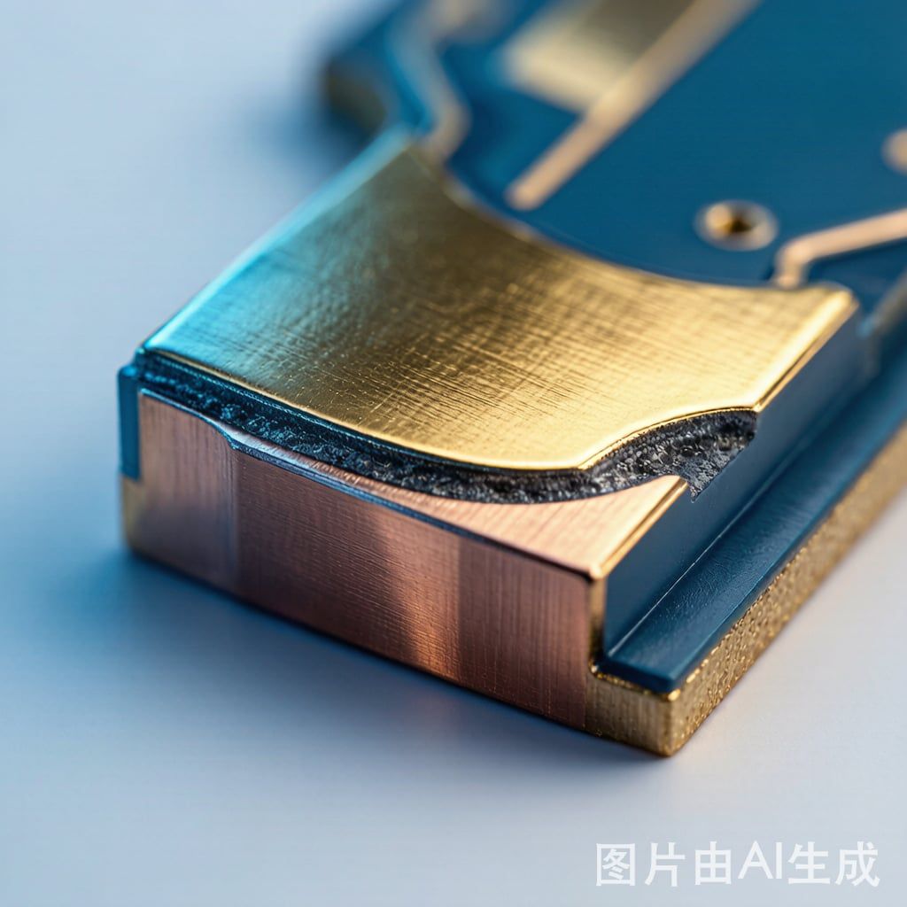
Electroless Nickel Immersion Gold (ENIG) has become one of the most widely used surface finishes in PCB manufacturing, especially for fine-pitch SMT assembly. At the heart of ENIG’s reliability story is the nickel barrier layer — a thin but critically important electroless nickel-phosphorus deposit that sits between the copper pad and the immersion gold top layer.
Without this nickel barrier, copper atoms would rapidly diffuse into the gold layer, forming brittle copper-gold intermetallic compounds (IMCs) that compromise solder joint integrity. The nickel layer acts as a physical and chemical diffusion barrier, ensuring that the solder bonds to a clean, predictable surface.
Electroless Nickel: Composition and Deposition
The electroless nickel layer used in ENIG is not pure nickel — it is a nickel-phosphorus (Ni-P) alloy containing 6-10% phosphorus by weight. This phosphorus content is crucial because it creates an amorphous or nanocrystalline structure that effectively blocks diffusion paths for copper atoms.
Key characteristics of the nickel barrier layer:
- Thickness: Typically 3-7 μm (IPC-4552 specifies 3-6 μm minimum)
- Phosphorus content: Mid-phosphorus (6-9%) is most common; high-phosphorus (10-12%) offers better corrosion resistance
- Deposition method: Autocatalytic chemical reduction using sodium hypophosphite
- Porosity: Must be extremely low to prevent copper migration pathways
The Black Pad Problem and Nickel Corrosion
One of the most infamous failure modes in ENIG is black pad syndrome, where excessive nickel corrosion occurs during the immersion gold plating step. When the gold bath chemistry is too aggressive or phosphorus content is too low, the nickel surface becomes pitted and oxidized, leading to brittle solder joints that fracture under mechanical stress.
Prevention strategies include:
- Maintaining phosphorus content at 7-9% for optimal corrosion resistance
- Controlling immersion gold bath pH, temperature, and dwell time
- Adding trace amounts of stabilizers to the gold bath
- Performing regular cross-section analysis for quality control
ENEPIG: Adding Palladium for Enhanced Protection
Electroless Nickel Electroless Palladium Immersion Gold (ENEPIG) evolved as a direct response to the limitations of ENIG. By adding an electroless palladium layer (0.05-0.15 μm) between the nickel and gold, ENEPIG solves several critical problems:
- The palladium layer prevents nickel corrosion during gold deposition entirely
- Palladium acts as an additional diffusion barrier
- Solder wetting is more uniform and reliable
- Wire bonding performance (for IC packages) is significantly improved
- Compatible with both Sn-Pb and lead-free solders
Intermetallic Formation and Solder Joint Reliability
During reflow soldering, the solder interacts with the surface finish to form IMCs at the interface. With ENIG, the dominant IMC is Ni₃Sn₄, which forms when tin in the solder reacts with the nickel layer after the thin gold layer dissolves into the molten solder.
The nickel barrier layer must be thick enough to survive multiple reflow cycles without being fully consumed. IPC-4552 specifies a minimum nickel thickness of 3 μm, which provides adequate margin for up to three reflow cycles plus subsequent field operating conditions.
Best Practices for ENIG Process Control
To ensure reliable nickel barrier performance, PCB fabricators and quality engineers should:
- Monitor phosphorus content in each plating batch using XRF or ICP analysis
- Perform solderability testing per J-STD-003 on every lot
- Conduct cross-sectional SEM/EDS analysis for nickel thickness and morphology
- Implement statistical process control (SPC) for gold bath parameters
- Use accelerated aging tests (e.g., steam aging) to validate long-term reliability
When properly executed, the nickel barrier layer in ENIG and ENEPIG provides a robust, reliable surface finish that supports the demanding requirements of modern SMT assembly.


