The Rise of Ni-Pd-Au Lead Finishes in SMT
Nickel-palladium-gold (Ni-Pd-Au) lead finishes have become increasingly prevalent in SMT electronics, driven by the global shift away from tin-lead (Sn-Pb) plating and the reliability concerns associated with pure matte tin finishes. Tin whiskers — conductive filaments that grow from pure tin surfaces — remain a serious reliability risk in high-reliability applications, particularly aerospace, medical, and automotive electronics. Ni-Pd-Au provides a whisker-mitigated, solderable surface without requiring tin.
Major semiconductor manufacturers including NXP, Infineon, ON Semiconductor, and Texas Instruments now offer extensive product lines with Ni-Pd-Au lead finishes. However, this finish behaves differently from traditional tin or tin-lead during reflow soldering, requiring specific reflow profile optimization to achieve reliable solder joints.
The key challenges with Ni-Pd-Au are: (1) palladium and gold dissolution into the solder alloy alters the solder’s microstructure and mechanical properties; (2) the dissolution rate is strongly temperature-dependent, making peak temperature control critical; (3) wetting behavior differs from tin-based finishes, requiring adjusted soak times and temperatures; and (4) gold embrittlement can occur if the gold concentration in the solder joint exceeds safe limits.
This article provides practical guidance for optimizing SMT reflow profiles to achieve reliable solder joints with Ni-Pd-Au finished components.
Understanding Ni-Pd-Au Finish Structure and Soldering Behavior
A typical Ni-Pd-Au lead finish consists of three layers over the copper or copper-alloy lead frame:
Nickel Underplate: 1.5-5.0 μm of electrolytic or electroless nickel. Serves as a diffusion barrier preventing copper-zinc migration from the base metal and provides a stable substrate for the precious metal layers. The nickel layer remains intact during soldering and forms the Ni-Sn intermetallic compound (IMC) that bonds the solder to the lead.
Palladium Layer: 0.1-0.5 μm of palladium. Provides the primary whisker mitigation function and serves as a solderable surface. Palladium dissolves rapidly into molten solder — approximately 10× faster than nickel at reflow temperatures — and forms Pd-Sn intermetallic compounds within the solder joint. Excessive palladium dissolution can create brittle PdSn₄ intermetallic plates that degrade joint mechanical properties.
Gold Flash: 0.003-0.05 μm (3-50 nm) of gold. An extremely thin protective layer that prevents palladium oxidation and tarnishing during storage, ensuring consistent solderability. At this thickness, the gold contribution to joint composition is negligible (well below the 3 wt% Au embrittlement threshold).
Dissolution Sequence During Reflow: When the solder paste melts and contacts the Ni-Pd-Au surface, dissolution occurs in sequence: (1) the ultra-thin gold flash dissolves almost instantly (within 1-2 seconds) at temperatures above 200°C; (2) the palladium layer dissolves more gradually over 30-90 seconds depending on temperature; (3) once the palladium is consumed, the solder contacts the nickel underplate and forms the Ni₃Sn₄ or NiSn IMC bond.
Gold Embrittlement: The Critical Design Constraint
Gold embrittlement is the primary metallurgical concern when soldering to gold-bearing surfaces. When gold dissolves into solder, it forms AuSn₄ intermetallic plates that are brittle and can create crack initiation sites under thermal or mechanical stress:
The 3 wt% Rule: Industry consensus (IPC J-STD-001, IPC-7095) limits gold concentration in the final solder joint to 3 wt% maximum. Above this threshold, AuSn₄ plate formation becomes excessive, and joint ductility and fatigue life degrade significantly. For critical applications (Class 3 per IPC-A-610), the limit is reduced to 2 wt%.
Gold Concentration Calculation: The gold concentration in the solder joint depends on the gold volume (thickness × area) relative to the solder volume. For Ni-Pd-Au finished components with a gold flash of 0.003-0.05 μm, the gold contribution is typically < 0.1 wt% in the solder joint — well below the embrittlement threshold. This is a key advantage of Ni-Pd-Au over thicker gold-plated contacts (which may have 0.5-1.27 μm gold).
Palladium Concentration Concern: While less well-documented than gold embrittlement, excessive palladium in solder (>5 wt%) can form brittle PdSn₄ intermetallic plates that similarly degrade joint reliability. For Ni-Pd-Au components with palladium thickness of 0.1-0.5 μm, the palladium concentration in typical solder joints is 0.1-1.0 wt%, which is within acceptable limits. However, components with thicker palladium (>0.5 μm) combined with small solder volumes may approach the problematic concentration range.
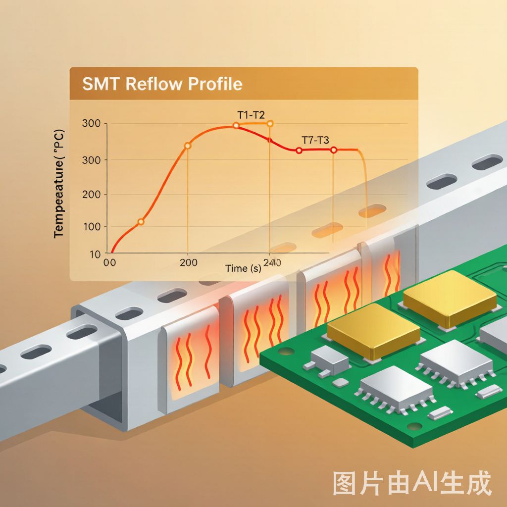
Optimizing the Reflow Profile for Ni-Pd-Au
The reflow profile — the time-temperature curve that the assembly follows through the reflow oven — must be adjusted for Ni-Pd-Au’s specific wetting and dissolution characteristics:
Ramp-to-Soak Zone (25°C to 150-170°C): A moderate ramp rate of 1-2°C/second is recommended. This is the same as for standard SAC305 reflow. The goal is to activate the flux, evaporate solvents, and bring the entire assembly to a uniform temperature before entering the soak zone. Avoid ramp rates above 3°C/second, which can cause solder paste splattering and component thermal shock.
Soak Zone (150-170°C to 200-210°C, 60-120 seconds): The soak zone serves a critical function for Ni-Pd-Au finishes. The palladium layer requires time to dissolve into the solder, and the soak ensures that dissolution begins gradually before the peak temperature is reached. A soak temperature of 170-200°C for 60-90 seconds provides adequate time for palladium to begin dissolving and for the solder to wet the lead surface. Too short a soak ( 150 seconds) risks excessive palladium dissolution and flux depletion before reaching peak temperature.
Peak Zone (230-245°C, 30-90 seconds above 217°C): The peak temperature must be high enough to fully melt the SAC305 solder (liquidus 217°C) and form a robust Ni-Sn IMC, but not so high that palladium dissolution becomes excessive. A peak temperature of 235-245°C with 40-70 seconds above 217°C (time above liquidus, TAL) is recommended for Ni-Pd-Au finished components. This provides sufficient thermal energy for reliable IMC formation while limiting palladium dissolution to acceptable levels.
Cooling Zone (peak to 200°C, then to ambient): A controlled cooling rate of 1-3°C/second through the solidification range produces a fine-grained solder microstructure with better mechanical properties. Avoid cooling rates above 4°C/second, which can create thermal stress in the solder joints and the component packages.
Wetting Behavior and Solder Paste Selection
Ni-Pd-Au surfaces exhibit different wetting characteristics compared to tin or tin-lead finishes:
Wetting Speed: Palladium surfaces wet more slowly than tin or tin-lead surfaces. The solder must first dissolve the gold flash and then the palladium layer before contacting the nickel underplate and forming the IMC bond. This means the wetting time for Ni-Pd-Au is typically 0.5-2.0 seconds longer than for tin-plated leads at the same temperature. The extended soak zone in the reflow profile compensates for this slower wetting.
Solder Paste Compatibility: SAC305 (Sn-3.0Ag-0.5Cu) and SAC405 (Sn-4.0Ag-0.5Cu) solder pastes are fully compatible with Ni-Pd-Au finishes. No special paste formulation is required. However, the flux system must be active enough to reduce the palladium oxide that can form during storage — particularly for components that have been stored for extended periods in humid environments. No-clean flux formulations with moderate-to-high activity (ROL0 or ROL1 per J-STD-004) are recommended.
Wetting Test Verification: Per IPC J-STD-002, perform a dip-and-look wetting test on incoming Ni-Pd-Au finished components, particularly for lots with unknown storage history. The solder should wet the lead surface within 2-3 seconds at 235°C, with at least 95% coverage. Components failing the wetting test may require pre-ti
ing or may be contaminated with oxidation or organic residues that the standard flux ca
ot remove.
Common Defects and Troubleshooting
Ni-Pd-Au finished components can exhibit specific soldering defects that differ from tin-plated components:
Non-Wetting on Palladium: If the solder does not fully dissolve the palladium layer, the remaining Pd acts as a barrier preventing the solder from bonding to the nickel. The joint appears soldered but has poor mechanical strength. Cause: insufficient peak temperature or TAL. Solution: increase peak temperature by 5-10°C or extend TAL by 10-20 seconds.
Dewetting After Initial Wetting: The solder initially wets the Pd-Au surface but then retreats, leaving irregular patches of exposed palladium. Cause: excessive oxidation of the palladium surface from prolonged storage or improper packaging. Solution: use a more active flux, pre-tin the leads, or reject the affected lot.
Brittle Fracture at IMC Interface: The solder joint fractures at the Ni-Sn IMC layer under mechanical stress, rather than through the bulk solder. Cause: excessive PdSn₄ intermetallic formation from over-dissolution of palladium, or too-thin nickel underplate allowing Cu-Sn IMC formation. Solution: reduce peak temperature or TAL, verify component plating thickness per specification, and ensure the nickel barrier is at least 1.5 μm thick.
Voiding Under Component Leads: Higher voiding rates have been reported for some Ni-Pd-Au finished components compared to tin-plated equivalents. Cause: the rapid dissolution of the thin gold flash can generate outgassing, and the palladium dissolution process may trap flux volatiles. Solution: use a longer soak to allow volatiles to escape before the solder melts, and ensure the reflow profile provides adequate time above liquidus for void reduction.
Profile Validation and Process Control
Validating the reflow profile for Ni-Pd-Au components requires specific checks beyond standard SAC305 profiling:
Profile Measurement: Attach thermocouples directly to Ni-Pd-Au finished leads (not to the PCB pad) to measure the actual lead temperature during reflow. The lead temperature determines the Pd dissolution rate and IMC formation — not the PCB temperature. Use high-temperature solder or thermally conductive adhesive to attach thermocouples.
Cross-Sectional Analysis: For initial profile qualification, cross-section 5-10 solder joints from a production run and examine under 200-500× magnification. Verify: (1) complete dissolution of the Pd-Au layer (no visible residual Pd at the interface); (2) a uniform, continuous Ni-Sn IMC layer (1-3 μm thick); (3) no excessive PdSn₄ intermetallic plates in the bulk solder; (4) acceptable voiding (< 25% of joint area per IPC-A-610 Class 2).
Process Window: Establish a process window for peak temperature and TAL based on cross-sectional analysis results. The window should provide a margin of at least ±5°C and ±10 seconds from the nominal profile settings to accommodate oven-to-oven and run-to-run variations.
Conclusion
SMT reflow profile optimization for Ni-Pd-Au lead finish components requires attention to the unique dissolution and wetting behavior of the palladium layer. The key adjustments compared to standard tin-plated component reflow are: an extended soak zone (60-90 seconds at 170-200°C) to promote gradual palladium dissolution and ensure complete wetting; a controlled peak temperature (235-245°C) and TAL (40-70 seconds) that balance IMC formation against excessive palladium dissolution; and careful verification through cross-sectional analysis during initial profile qualification.
With properly optimized reflow profiles, Ni-Pd-Au finished components produce solder joints with reliability equivalent to or better than tin-plated alternatives, while eliminating the tin whisker risk that makes pure tin finishes problematic for high-reliability applications. The investment in profile optimization pays dividends through consistent solder joint quality, reduced defect rates, and compliance with whisker-mitigation requirements in automotive, aerospace, and medical electronics manufacturing.


