Why Copper Trace Current Capacity Matters in PCB Design
Every PCB designer faces the same fundamental question when routing power traces: how wide does this copper trace need to be to carry the required current safely? An undersized trace will overheat, potentially delaminating from the FR-4 substrate, burning open like a fuse, or degrading over time through electromigration. An oversized trace wastes valuable board real estate that could be used for additional routing or component placement.
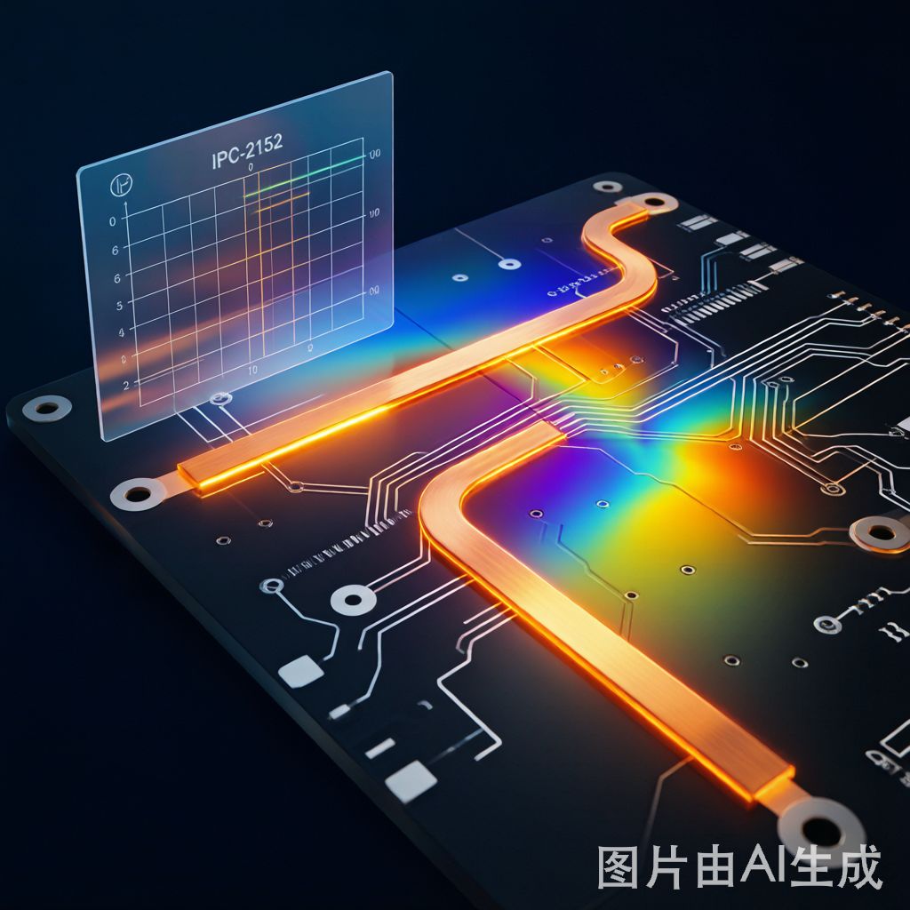
The answer to this question has been standardized in IPC-2152, “Standard for Determining Current-Carrying Capacity in Printed Board Design,” which replaced the decades-old IPC-2221 charts with a more scientifically rigorous methodology based on actual thermal testing. IPC-2152 accounts for variables that the old charts ignored: copper plane area, board thickness, and the presence of parallel conductors that preheat the surrounding board material.
For SMT PCB designers working with copper traces — whether for power distribution in server backplanes, high-current motor drives, or densely packed consumer electronics — understanding IPC-2152 is essential for designing reliable, thermally sound boards. This guide covers the practical application of IPC-2152, with worked examples and design rules specific to SMT assemblies.
IPC-2152 vs IPC-2221: What Changed and Why
The transition from IPC-2221 to IPC-2152 represents a fundamental improvement in trace current capacity methodology:
IPC-2221 Limitations: The old charts were derived from a limited set of empirical tests conducted in the 1950s on single traces on simple test boards. They did not account for the thermal effects of copper planes (which act as heat spreaders), adjacent heated traces, or varying board thickness. The charts also assumed a single ambient temperature (typically 20°C) and required designers to apply arbitrary derating factors for real-world conditions.
IPC-2152 Improvements: Based on extensive thermal testing conducted in the early 2000s, IPC-2152 provides a physics-based model that accounts for: cross-sectional area of the conductor (not just width); thermal conductivity of the dielectric material; proximity of copper planes (internal vs external layers); board thickness; and the presence of adjacent heated conductors. Most importantly, IPC-2152 recognizes that internal traces on layers adjacent to copper planes carry significantly more current than traces on layers far from a thermal plane for the same temperature rise.
The Key Insight: A trace’s current capacity is fundamentally limited by its operating temperature, which is determined not just by I²R heating in the trace itself, but by how efficiently that heat can be conducted away through the PCB dielectric to copper planes and ultimately to the ambient environment. This explains why the same trace cross-section on different board constructions has very different current ratings.
Understanding the IPC-2152 Current-Capacity Charts
IPC-2152 presents current capacity data in chart form, parameterized by key design variables:
Conductor Cross-Sectional Area: The fundamental parameter on the horizontal axis of IPC-2152 charts. Cross-sectional area = trace width × copper thickness. For example, a 2.0mm wide trace with 1 oz (35μm) copper has a cross-section of 0.070 mm². Doubling copper weight from 1 oz to 2 oz doubles the cross-section for the same width, effectively doubling the current capacity.
Temperature Rise (ΔT): The allowable temperature increase above ambient, typically 10°C, 20°C, or 30°C. IPC-2152 provides separate curves for each ΔT. A trace operating at 30°C rise carries substantially more current than a trace limited to 10°C rise, but the higher operating temperature may affect nearby components and reduce board life.
Internal vs External Layers: External traces (on the outer layers of the PCB) benefit from convection and radiation cooling to ambient air, allowing approximately 1.5-2× the current capacity of internal traces with the same cross-section and ΔT. However, external traces are also subject to solder mask coverage, which reduces convective cooling by 10-20%.
Plane Proximity Effect: Internal traces on layers adjacent to a solid copper plane (0.1-0.2mm dielectric thickness) carry approximately 1.2-1.5× the current of traces far from a plane, because the plane acts as an effective heat spreader. This thermal coupling is one of the most significant improvements of IPC-2152 over IPC-2221.
Practical Trace Width Calculation Examples
The following examples illustrate IPC-2152 calculations for common SMT PCB scenarios using 1 oz (35μm) copper:
Example 1: 5A Power Trace, External Layer, 20°C Rise
From IPC-2152 external conductor charts, 5A at 20°C rise requires approximately 1.0 mm² cross-section. With 35μm copper thickness: Width = 1.0 / 0.035 = 28.6mm. This is clearly impractical on a dense PCB. Options: increase copper weight to 2 oz (70μm, width = 14.3mm) or allow 30°C rise (width ≈ 10mm with 1 oz copper, 5mm with 2 oz). For most designs, 2 oz copper on external power layers is the preferred solution for currents above 3A.
Example 2: 2A Internal Trace, Adjacent to Ground Plane, 10°C Rise
With plane proximity advantage (approximately 1.3× for adjacent layer): 2A at effective 10°C rise requires approximately 0.40 mm² with the proximity factor applied. Width = 0.40 / 0.035 = 11.4mm. This trace occupies significant route space but ensures reliable operation with minimal temperature rise for sensitive analog or precision circuits.
Example 3: 500mA Signal Trace, External Layer, 10°C Rise
A 500mA trace at 10°C rise requires only 0.15 mm² cross-section. Width = 0.15 / 0.035 = 4.3mm with 1 oz copper. While seemingly wide for a “signal” trace, this demonstrates that any trace carrying more than a few hundred milliamps deserves careful sizing consideration.
Practical Rule of Thumb for 1 oz Copper on External Layers at 20°C Rise: 1A per mm of trace width for traces 1-5mm wide on standard FR-4 with moderate copper plane area. This is a conservative approximation; actual IPC-2152 capacity is slightly higher, particularly for narrow traces.
Thermal Management for High-Current SMT Traces
When trace width alone ca
ot meet current requirements within available board space, several design techniques can manage thermal performance:
Copper Weight Increase: Moving from 1 oz to 2 oz copper doubles the cross-section for the same trace width, effectively doubling the current capacity. 3 oz and 4 oz copper are available for extreme current applications (power supplies, motor controllers). However, heavy copper increases etching undercut and minimum trace/space requirements, complicating fine-pitch SMT routing.
Solder Mask Openings: Removing solder mask over high-current traces and applying solder (typically during wave soldering or selective soldering) adds significant copper-equivalent cross-section. A trace with a solder buildup of 0.1-0.2mm thickness over 35μm copper has effectively 3-6× the current capacity of the bare trace. This technique is widely used in power supply PCBs.
Parallel Traces on Multiple Layers: Instead of one wide trace, route the current through parallel traces on multiple layers co
ected by a matrix of vias. Two 5mm traces (one on top, one on bottom) effectively double the current capacity compared to a single 5mm trace, assuming good via stitching for current sharing.
Bus Bar Integration: For currents above 20-30A, soldering a bare copper bus bar (a thick copper strip) to the PCB alongside or on top of the trace provides massive current capacity in minimal board area. Bus bars 2-5mm thick × 5-20mm wide can carry 100-500A with minimal temperature rise.
Thermal Via Arrays: For internal traces carrying high current to power planes, thermal vias (arrays of plated through-holes) conduct heat from the trace to external layers or internal planes. A 5×5 array of 0.3mm vias on 1.0mm pitch can reduce the thermal resistance from an internal trace to an external heatsink by 50-70%.
Temperature Rise Limits for SMT PCB Reliability
Selecting the appropriate temperature rise limit is as important as calculating the trace width:
FR-4 Temperature Limits: Standard FR-4 has a glass transition temperature (Tg) of 130-140°C. Continuous operation above 110°C accelerates delamination and reduces board life. For commercial electronics, limit total trace temperature to 105°C maximum (allowing approximately 60°C rise above 45°C ambient). For automotive and industrial, high-Tg FR-4 (Tg 170-180°C) is recommended.
Component Proximity Effects: High-current traces generate heat that affects nearby SMT components. A trace at 30°C rise with 0.5mm spacing to an electrolytic capacitor reduces the capacitor’s life by 50% compared to operation at ambient temperature, per the Arrhenius equation (life halves for every 10°C increase). Route high-current traces at least 3-5mm from temperature-sensitive components.
Reliability Standards: IPC-2152 recommends 10°C rise for general applications, 20°C rise for applications where some heating is acceptable, and up to 30°C rise for applications where maximum current capacity in limited space is the primary requirement. Military and aerospace applications typically specify 10°C rise or less.
Conclusion
IPC-2152 provides PCB designers with a scientifically validated, practical methodology for determining copper trace current capacity. By accounting for copper plane proximity, board construction, and the physics of heat conduction through PCB materials, it enables more accurate and often more compact trace designs than the legacy IPC-2221 charts.
For SMT PCB designers, the key practical takeaways are: use the plane proximity advantage for internal power layers, consider increasing copper weight for high-current traces above 3A, and always account for the thermal impact of high-current traces on nearby temperature-sensitive components. A trace that meets its IPC-2152 electrical requirements but cooks an adjacent electrolytic capacitor is not a successful design.
IPC-2152 reminds us that current capacity is fundamentally a thermal problem, not an electrical one. Designing for safe temperature rise — considering both the trace and its thermal environment — is the path to reliable, long-life SMT PCB assemblies.


