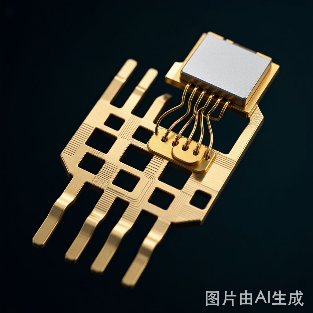
The Role of Lead Frames in Semiconductor Packaging
The lead frame is the structural backbone of virtually every wire-bonded semiconductor package. It provides the mechanical support for the silicon die, the electrical interco
ection between the die and the printed circuit board, and the thermal path for heat dissipation from the active junction to the external environment. In the global semiconductor supply chain — where billions of packages are produced monthly — the lead frame material directly determines package performance, reliability, and manufacturing cost.
Brass (copper-zinc alloy) has been a mainstream lead frame material for decades, particularly for consumer-grade and mid-range semiconductor packages. It offers a compelling balance of electrical conductivity, thermal performance, formability, and cost that makes it the material of choice for TO-series discrete packages, DIP (Dual In-line Package), and many SOP (Small Outline Package) variants.
However, as semiconductor packaging evolves toward thi
er profiles, higher power densities, and more demanding thermal requirements, the selection of lead frame material has become increasingly nuanced. This article examines brass lead frames in detail — their properties, advantages, limitations, and optimal application spaces — to help packaging engineers make informed material decisions.
Brass Alloys Commonly Used in Lead Frames
Not all brass alloys are suitable for lead frame applications. The alloy must simultaneously satisfy electrical, thermal, mechanical, and manufacturing requirements:
C19400 (Copper-Iron, 97.5Cu-2.35Fe-0.03P-0.12Zn): While technically a copper-iron alloy rather than a true brass, C194 is the most widely used lead frame material globally. Its exceptional combination of high thermal conductivity (260 W/m·K), moderate electrical conductivity (65% IACS), high tensile strength (450-550 MPa in half-hard condition), and excellent stress relaxation resistance makes it the standard for DIP, SOP, and QFP packages. The iron addition provides precipitation hardening and controls grain size.
C19200 (Copper-Iron-Phosphorus, 98.9Cu-1.0Fe-0.03P): Similar to C194 but with lower iron content. Thermal conductivity is slightly higher (265 W/m·K) with marginally lower strength (400-500 MPa half-hard). Used where maximum thermal performance is needed within the copper-iron alloy family.
C26800 (Yellow Brass, 66Cu-34Zn): The most common true brass alloy used for lead frames in cost-sensitive applications. Electrical conductivity is 27% IACS and thermal conductivity is approximately 120 W/m·K — significantly lower than C194 but adequate for low-power packages. Tensile strength in half-hard condition is 420-510 MPa. The primary advantage is material cost, which is 30-50% lower than C194.
C26000 (Cartridge Brass, 70Cu-30Zn): Higher copper content provides slightly better conductivity (28% IACS) and formability than C26800, with marginally higher material cost. Used for lead frames requiring more severe forming operations (tight bends, deep draws) where C26800 may crack.
C70250 (Copper-Nickel-Silicon, Cu-3.0Ni-0.65Si-0.15Mg): A high-performance alloy increasingly used as a C194 replacement for advanced packages. Corson-type precipitation hardening achieves very high strength (600-750 MPa) while maintaining good conductivity (35-45% IACS). Superior stress relaxation resistance at elevated temperatures makes it suitable for automotive and high-reliability applications.
Thermal Performance: Brass vs Alternative Lead Frame Materials
Thermal conductivity is a critical lead frame specification because the lead frame is often the primary heat conduction path from the die to the PCB:
Thermal Conductivity Comparison:
• Oxygen-Free Copper (C10200): 360-390 W/m·K
• C19400 (Cu-Fe): 260 W/m·K
• C70250 (Cu-Ni-Si): 180-220 W/m·K
• C26800 (Yellow Brass): 115-120 W/m·K
• Alloy 42 (Fe-42Ni): 14-16 W/m·K
• Kovar (Fe-29Ni-17Co): 17 W/m·K
The thermal advantage of copper-based alloys (including brass) over iron-nickel alloys (Alloy 42, Kovar) is dramatic — approximately 7-25× higher thermal conductivity. This makes brass and copper alloys essential for power semiconductor packages where junction temperature must be kept below 150°C for reliable operation.
However, the thermal advantage must be weighed against the CTE mismatch penalty. Brass CTE (approximately 20 ppm/°C for C26800) is significantly higher than silicon CTE (2.6 ppm/°C), creating a large CTE gap that can cause die attach delamination and solder fatigue in power cycling. Alloy 42 (CTE ~4.5 ppm/°C) closely matches silicon and is preferred for hermetic and high-reliability packages despite its poor thermal conductivity.
Manufacturing: Stamping vs Photochemical Etching
Lead frames are manufactured by two primary processes, each with distinct cost and capability profiles:
Progressive Die Stamping: The dominant manufacturing method for high-volume lead frames. A coil of brass or copper alloy strip is fed through a multi-station progressive die that punches, forms, and coines the lead frame in a single pass. Typical production rates: 200-600 strokes per minute. Stamping is extremely cost-effective at high volumes (>$100K tooling amortized over millions of units), achieving unit costs of $0.001-0.01 per lead frame for standard packages.
Key stamping considerations for brass lead frames: C26800 and C26000 have excellent formability for the bending and coining operations in the die. Strip thickness is typically 0.15-0.25mm for SOP packages and 0.25-0.50mm for power packages. Strip cleanliness and surface finish are critical — oil residue, scratches, or surface defects cause plating adhesion failures and wire bond quality issues.
Photochemical Etching (Milling): Used for prototype and low-to-medium volume production where stamping tooling cost ca
ot be justified. A photoresist pattern is applied to the brass strip, and chemical etching removes the unwanted material. Etching achieves finer features than stamping (down to 0.05mm line/space) and produces burr-free edges that improve plating uniformity. Unit costs are 5-20× higher than stamping for equivalent geometries.
Etching is also preferred for packages with very fine lead pitches (< 0.4mm) where the mechanical forces of stamping would distort the delicate leads. Many QFP and TQFP lead frames with 0.3mm lead pitch are produced by etching even at high volumes.
Plating Requirements for Brass Lead Frames
Brass contains zinc, which migrates to the surface and forms insulating oxide layers that prevent reliable wire bonding and soldering. All brass lead frames require surface plating:
Silver Spot Plating: Selective silver plating (3-8 μm) applied only to the die pad and wire bond finger areas. Silver provides excellent wire bondability (both gold and aluminum wire) and is the standard plating for wire-bonded packages. The plating is applied by selective immersion or brush plating, leaving the rest of the lead frame unplated to control cost.
Pre-Plated Lead Frames (PPLF): The entire lead frame is plated in coil form before stamping, typically with a nickel barrier layer (1-3 μm) followed by a thin palladium flash (0.02-0.10 μm) and a gold flash (0.01-0.03 μm). PPLF eliminates the need for post-stamping plating and provides excellent solderability for surface mount assembly. The nickel barrier prevents zinc migration through the plating layers.
Post-Mold Plating (Sn/Pb or Matte Sn): After transfer molding and deflashing, the external leads are plated with solder (traditionally Sn/Pb, now matte tin for RoHS compliance) to ensure solderability during PCB assembly. The plating covers only the external lead portions, not the die pad or bond fingers.
Zinc Migration Prevention: For brass lead frames, the nickel barrier layer is critical. Without it, zinc from the brass substrate migrates through the silver or gold plating to the surface within weeks at room temperature, forming zinc oxide that destroys wire bondability. The nickel barrier must be at least 1.0 μm thick, and 2.0 μm is recommended for packages that may be stored for extended periods before assembly.
Reliability Considerations
Brass lead frame packages face specific reliability challenges that packaging engineers must address:
Stress Relaxation: At elevated operating temperatures (125°C+), brass lead frames lose a portion of their clamping force on the molding compound, potentially leading to package delamination. C19400 and C70250 alloys have significantly better stress relaxation resistance than C26800, retaining >80% of their initial stress after 1,000 hours at 150°C versus 50-60% for yellow brass.
Moisture Sensitivity: The higher CTE of brass compared to Alloy 42 or copper means greater thermal mismatch with the molding compound during reflow soldering. This can cause interfacial delamination (popcorning) in moisture-sensitive packages. MSL (Moisture Sensitivity Level) ratings for brass lead frame packages are typically one level worse than equivalent Alloy 42 packages.
Corrosion Resistance: Brass is susceptible to dezincification — selective leaching of zinc — in humid, slightly acidic environments. This weakens the lead frame over time and can cause lead breakage. Nickel or tin plating on the external leads provides adequate protection for most applications, but bare brass internal surfaces (die pad underside, between leads) remain vulnerable in harsh environments.
Conclusion
Brass lead frames — particularly C26800 and C26000 alloys — remain economically viable for cost-sensitive semiconductor packages where moderate thermal and electrical performance is acceptable. However, for power semiconductors, high-temperature applications, and advanced packages requiring fine pitch or superior reliability, copper-iron (C194) and copper-nickel-silicon (C70250) alloys are increasingly the materials of choice despite their higher cost.
The lead frame material decision is ultimately a system-level trade-off among thermal performance, CTE compatibility, mechanical reliability, and cost. For packaging engineers, understanding the full performance envelope of each alloy — beyond just cost and conductivity — is essential for designing semiconductor packages that meet their reliability targets over the intended product lifetime.


