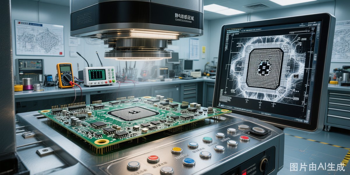
X-ray inspection (AXI — Automated X-ray Inspection) has become indispensable in modern SMT assembly for one simple reason: BGA, LGA, QFN, and CSP packages have solder joints that are completely hidden under the component body and physically inaccessible to optical inspection. X-ray sees through everything.
How X-Ray Inspection Works
X-ray systems direct a focused X-ray beam at the PCB assembly. Dense materials like solder (containing tin, lead, or silver) absorb X-rays and appear dark in the image. Air voids appear bright. The system captures either 2D images or, in more advanced systems, 3D tomographic slices (CT-style) that allow inspection of individual solder ball layers independently.
Defects Detectable by X-Ray
- BGA/CSP voiding: Gas bubbles trapped in solder balls — IPC-7095 specifies acceptable void percentages by application class
- Bridges (shorts): Solder co
ections between adjacent balls or pads not visible optically
- Missing solder balls: Completely absent joints that ca
ot be detected by any other method
- Head-in-pillow (HIP): Ball and paste do not fully coalesce — appears as a distinct interface line in X-ray images
- Cold joints: Irregular, grainy solder ball morphology indicating incomplete reflow
- QFN thermal pad opens: Incomplete wetting under QFN thermal pads affecting both electrical and thermal performance
2D vs 3D X-Ray: When Each is Needed
2D X-ray projects all layers into a single image — fast and cost-effective, but complex boards with multiple component layers create overlapping images that are difficult to interpret. 3D X-ray (AXI with CT capability) reconstructs cross-sectional slices, enabling precise defect localization and accurate void percentage measurement in individual BGA solder balls. 3D is strongly recommended for complex assemblies with boards above 4 layers and dense component placement.
IPC-7095 Voiding Acceptance Criteria
IPC-7095D provides the industry standard for BGA design and assembly. For void acceptance, Class 1 (General Electronics) allows voids up to 30% area per ball, Class 2 (Dedicated Service) allows up to 25% per ball, and Class 3 (High Reliability, used in automotive and aerospace) restricts voids to 15% per ball maximum.
Thermal interface balls (center pad in QFN packages) are often allowed higher void percentages up to 50% since they primarily serve thermal rather than electrical functions, and uniform voiding has minimal impact on thermal resistance.
Integrating X-Ray into the Production Flow
Inline AXI after reflow soldering provides 100% inspection coverage but requires significant capital investment ($150K-$500K for advanced systems). Offline X-ray (sample-based) is viable for prototypes, new product introduction, and periodic process audits. Many SMT lines use a hybrid approach: inline AOI for all boards, offline X-ray for BGA-heavy designs and all first-article inspections. This balances cost with detection coverage effectively.


