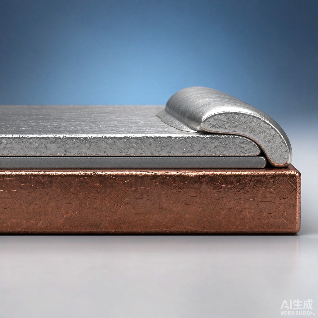
SMT copper strip used for stamped contacts, fuse clips, shield fingers, and battery co
ectors is frequently finished with a tin or tin-alloy plating to preserve solderability during storage and to provide a cost-effective alternative to gold or silver finishes. Tin plating thickness directly controls solderability shelf life, contact resistance, and the rate of intermetallic compound (IMC) growth at the copper-tin interface. Plating that is too thin fails to protect the copper substrate from oxidation and IMC penetration; plating that is too thick increases material cost, reduces fine-pitch formability, and can cause solder joint embrittlement through excessive Cu₆Sn₅ and Cu₃Sn growth. This article examines the engineering relationship between tin plating thickness, solderability shelf life, and reliability for SMT copper strip applications.
Tin Plating Types for SMT Copper Strip
Matte Tin vs Bright Tin
The two most common pure tin finishes differ in grain structure, appearance, and solderability behavior:
| Property | Matte Tin | Bright Tin |
|---|---|---|
| Crystal structure | Large columnar grains (0.5-5 µm) | Fine equiaxed grains with organic brighteners |
| Appearance | Dull gray, low reflectivity | Mirror-like, high reflectivity |
| Organic codeposit | <0.1 wt% carbon | 0.5-2.0 wt% carbon from brighteners |
| Solderability | Excellent, stable wetting | Good when fresh, can degrade with brightener outgassing |
| Whisker risk | Lower (large grains, compressive stress) | Higher (fine grains, high organic residue) |
| Typical applications | Press-fit, high-reliability contacts | Decorative, low-cost consumer parts |
For SMT copper strip, matte tin is generally preferred because the lower organic content reduces outgassing during reflow and the larger grain structure lowers tin whisker propensity under compressive stress from co
ector insertion or thermal cycling.
Intermetallic Growth and Shelf Life
Cu-Sn IMC Kinetics
From the moment tin is deposited on copper, interdiffusion creates Cu₆Sn₅ (η-phase) at room temperature and Cu₃Sn (ε-phase) after extended thermal exposure. The IMC layer grows according to a parabolic time law:
x = (k · t)0.5
where x is IMC thickness, k is the temperature-dependent growth rate constant, and t is time. At 25°C, Cu₆Sn₅ grows at approximately 0.001-0.003 µm/day; at 85°C/85% RH accelerated aging, the rate increases 10-50x. Once the total IMC thickness exceeds roughly 30-50% of the original tin thickness, solder wetting force and wetting time begin to degrade measurably.
| Tin Thickness (µm) | Storage at 25°C/60% RH | Storage at 40°C/90% RH | Reflow Cycles Survivable |
|---|---|---|---|
| 0.3 (flash tin) | 3-6 months | 2-4 weeks | 1x peak 245°C |
| 0.8-1.2 (standard) | 12-24 months | 3-6 months | 2-3x |
| 2.0-3.0 (heavy) | 36-60 months | 12-18 months | 4-6x |
| 5.0+ (hot tin dip) | 60-96 months | 24-36 months | 6-10x |
These values assume a clean matte tin deposit with a nickel underlayer of 1.0-2.5 µm. Without a nickel diffusion barrier, copper diffusion into tin is faster and shelf life is reduced by approximately 30-40% at elevated temperature.
Plating Thickness Selection by Application
Trade-offs for SMT Contact Types
Different SMT copper strip products require different tin thickness targets based on solder process, pitch, and environmental exposure:
| Application | Recommended Tin Thickness | Key Consideration |
|---|---|---|
| Fine-pitch stamped contacts (≤0.5 mm pitch) | 0.8-1.2 µm | Maintains edge definition and prevents solder bridging |
| Power contacts and busbar tabs | 2.0-5.0 µm | High current and multiple reflow cycles |
| Battery spring contacts | 1.5-3.0 µm | Wear + fretting + long shelf life |
| Press-fit compliant pins | 1.0-2.0 µm matte tin | Lubricity and stable insertion force |
| Shield fingers and grounding clips | 1.0-2.5 µm | Solderability after long warehouse storage |
For tropical Southeast Asian warehouses without climate control, selecting the upper end of each range is advisable. A 1.5 µm minimum specification rather than 0.8 µm provides a safety margin against the 80-95% relative humidity common during monsoon seasons.
Solderability Testing Standards
Wetting Balance and Dip Tests
Quantitative solderability assessment ensures tin-plated copper strip remains processable after storage:
- IEC 60368-2-69 / MIL-STD-202 Method 208: Wetting balance test measures wetting force (mN/mm) and time to reach 2/3 of maximum force; acceptable wetting time typically ≤1.0 s for SAC305 at 245°C.
- J-STD-002: Dip-and-look test with 8-hour steam aging preconditioning; classifies solderability by percentage of wettable area.
- DIN 32513: European wetting balance standard with defined specimen immersion speed and depth.
A shelf-life qualification program should test samples after 0, 6, 12, 24, and 36 months of storage under worst-case warehouse conditions. If wetting time exceeds 1.5 s or wetting force falls below 80% of the initial value, the material should be flagged for re-ti
ing or scrapped.
Storage and Handling Recommendations
Humidity and Contamination Control
Even a perfectly plated copper strip can lose solderability through improper storage:
- Moisture barrier bags: Use aluminum-laminated bags with desiccant and humidity indicator cards; maintain <10% RH inside sealed packaging.
- Temperature: Store at 15-25°C; avoid warehouse locations above 35°C where IMC growth accelerates.
- Handling: Wear lint-free gloves; skin oils and acidic fingerprints catalyze localized corrosion and cause dewetting during reflow.
- First-in-first-out (FIFO): Rotate inventory so material is used within 50% of rated shelf life.
- Re-ti
ing:
If shelf life is exceeded, chemical stripping and re-tiing can restore solderability for 30-50% of the cost of new material.
For SMT copper strip suppliers shipping into ASEAN markets, printing the plating date, alloy specification, and recommended use-by date on each reel enables electronics manufacturers to manage solderability inventory effectively and reduces line-down risk during high-volume production.



