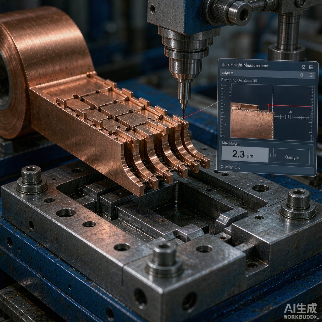
Why Edge Burr Quality Matters in SMT Copper Strip Contacts
In surface-mount assembly, copper strip contacts serve as spring fingers, shielding clips, busbar links, and thermal straps. These parts are stamped from rolled copper alloy strip at high speed, and the quality of the cut edge directly influences solder wetting, coplanarity, placement accuracy, and long-term contact reliability. A burr as small as 25 micrometers can lift a component off its pad, create solder voids, or short adjacent traces.
As SMT packages shrink to 0.4 mm pitch and below, the tolerance budget for edge defects tightens. IPC-A-610 Class 3 assemblies used in automotive and medical electronics demand burr heights below 10 percent of material thickness, and some OEMs impose even stricter limits of 5 percent. Meeting these requirements demands control over the entire stamping process, from die design to strip material specification.
Stamping Die Clearance and Burr Formation Mechanics
Burr formation is a natural consequence of the shear-cutting process. When the punch descends through the copper strip, three phases occur in sequence: elastic deformation, plastic deformation, and fracture. The fracture lines from the punch side and die side should meet cleanly; if they do not, a burr remains on the die-side edge.
The die clearance — the gap between punch and die — is the single most influential parameter. The recommended clearance for copper alloys is 4 to 8 percent of material thickness, with softer temper grades leaning toward the higher end to delay edge cracking.
Clearance Effects on Edge Quality
- Clearance too small (<3%): The fracture zones do not meet, producing a tall, thin burr and accelerated die wear. Edge hardening may also cause micro-cracks during forming.
- Clearance optimal (4-8%): Clean shear with minimal rollover (typically 10-20% of thickness), burnish depth of 30-50%, and burr height under 10 micrometers for 0.3 mm strip.
- Clearance too large (>10%): Excessive rollover and tear zone, producing a rough, feathery edge that catches on placement nozzles and guide rails.
For C26000 cartridge brass and C19400 Cu-Fe-P alloy strip at 0.2-0.5 mm thickness, a clearance of 0.012-0.030 mm (5-6%) typically yields the best edge quality. Softer temper grades (H01, H02) tolerate slightly larger clearances than harder tempers (H06, H08) because the fracture initiates more readily in harder material.
Measuring and Specifying Burr Height
Burr height is measured using optical profilometry or a precision micrometer with a flat anvil. The standard method is to sample five points along each cut edge and report the maximum value. For SMT contacts, the following limits are typical:
| Application Class | Max Burr Height | % of Thickness |
|---|---|---|
| Consumer electronics (Class 2) | 0.03 mm | 10% |
| Automotive / medical (Class 3) | 0.015 mm | 5% |
| Mil-aerospace (Class 3A) | 0.008 mm | 3% |
Specification drawings should reference the measurement method explicitly, because burr height can vary along the edge depending on tool wear progression. Tools typically produce acceptable burrs for 50,000 to 200,000 hits before requiring sharpening, depending on strip hardness and lubrication.
Deburring Methods for Copper Strip Contacts
When stamping alone ca
ot meet the burr specification, secondary deburring operations are required:
- Vibratory tumbling: Ceramic or plastic media in a vibratory bowl removes burrs from the strip edges. Cycle times of 10-30 minutes are typical for small contacts. The risk is over-processing, which rounds feature edges and alters contact geometry.
- Cryogenic deflashing: Parts are chilled to below -80 degrees C using liquid nitrogen, embrittling the burr, which is then removed by media blast. This method is fast and uniform but requires careful parameter tuning for thin copper sections.
- Brush deburring: Nylon-filament brushes with abrasive grit rotate against the strip to remove burrs directionally. Suitable for flat strip but not for complex-formed contacts.
- Electropolishing: A reverse-plating process that preferentially removes material from high points and burrs. It can reduce burr height by 50-80% while improving surface finish and solder wetting.
Material Selection for Burr-Sensitive Stamping
Strip temper and grain size affect burr behavior. Fine-grained material (ASTM grain size 0.015-0.025 mm) tends to produce cleaner fractures with lower burrs. C19400 and C70250 alloys in the precipitation-hardened condition offer good stampability with consistent edge quality. C26000 brass in H02 temper is the industry workhorse for general contacts, offering a good balance of formability, spring-back, and cost.
For high-volume SMT contact stamping, strip suppliers can provide edge-conditioned material with slit-edge burr controlled to under 5 micrometers, eliminating the need for secondary deburring on straight-cut features.
Impact on SMT Assembly and Solder Wetting
Burrs affect downstream assembly in several ways:
- Placement accuracy: A burr on the contact edge can prevent vacuum nozzle pickup or cause the part to sit at an angle, producing coplanarity defects.
- Solder wetting: Burrs create localized thick sections that delay solder wetting during reflow, and entrapped air in burr valleys can form voids under the joint.
- Contact resistance: Burrs on mating surfaces concentrate contact force on a small area, increasing initial contact resistance and accelerating fretting wear in vibration environments.
- Dendritic growth: Under bias and humidity, ionic contamination trapped in burr crevices can initiate electrochemical migration, reducing surface insulation resistance.
By controlling die clearance, monitoring tool wear, and specifying appropriate deburring when needed, manufacturers can consistently produce SMT copper strip contacts that meet Class 3 quality requirements while maintaining high stamping throughput and yield.



