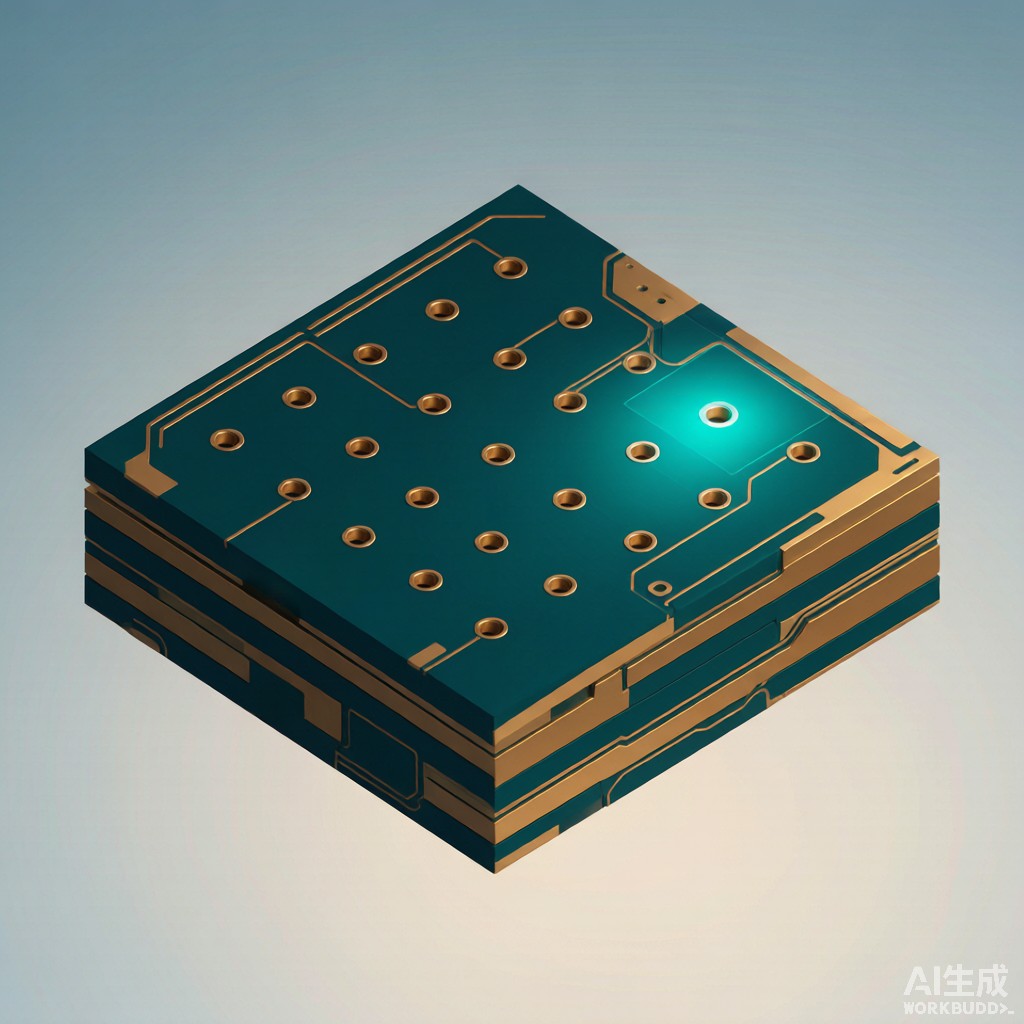
Mixed-signal IoT sensor modules integrate sensitive analog front-ends (sensors, ADCs, op-amps), high-speed digital sub-systems (microcontrollers, BLE/LoRa/Wi-Fi transceivers), and switching power converters on a single PCB. The proximity of sub-GHz sensor signals to multi-MHz digital clocks and RF transceivers operating in 2.4 GHz or sub-6 GHz 5G bands creates electromagnetic interference (EMI) coupling through PCB trace return paths, slot ante
as formed by ground plane splits, and common-mode radiation from co
ector cables. Proper PCB layer stackup design combined with stitching via fences around sensitive regions can achieve 25-40 dB EMI suppression at the PCB level, reducing or eliminating the need for additional external shielding cans. This article examines the engineering principles, stackup configurations, and stitching via design rules for mixed-signal IoT sensor modules.
PCB Stackup Fundamentals
Return Path and Impedance Control
Every high-frequency signal trace requires a continuous return path on the adjacent reference plane (ground or power). Discontinuities in this return path create ante
as that radiate and couple noise into adjacent traces:
- Microstrip (top layer trace over ground plane on layer 2): Returns on layer 2 ground; critical for >100 MHz signals.
- Stripline (i
er layer trace between two reference planes):
Spans between power and ground planes; lower radiation than microstrip. - Coplanar waveguide with ground: Returns on adjacent coplanar grounds; common for RF and 50-ohm controlled-impedance traces.
The ground plane must be a single continuous sheet under high-speed signals. Splits, gaps, or moats in the ground plane force return currents to detour around the gap, creating a loop ante
a that radiates with efficiency proportional to the loop area.
Layer Count Trade-Off Analysis
4-Layer vs 6-Layer vs 8-Layer Stackup
The choice of layer count directly affects EMI performance, signal integrity, and manufacturing cost:
| Stackup | Configuration | EMI Performance | Cost Index | Best Application |
|---|---|---|---|---|
| 2-layer | Sig / Gnd only | Poor (10-20 dB SE) | 1.0x | Sub-MHz sensor only, no RF |
| 4-layer | Sig / Gnd / Pwr / Sig | Moderate (25-35 dB SE) | 1.6-2.0x | Simple IoT, BLE only |
| 6-layer | Sig / Gnd / Sig / Gnd / Pwr / Sig | Good (40-55 dB SE) | 2.4-2.8x | Wi-Fi/BLE IoT, mixed-signal |
| 8-layer | Sig / Gnd / Sig / Gnd / Pwr / Sig / Gnd / Sig | Excellent (55-70 dB SE) | 3.5-4.2x | 5G FR1, mmWave FR2, multi-RF |
For sub-6 GHz 5G NR and Wi-Fi 6/6E IoT modules, a 6-layer stackup with two dedicated ground planes provides the optimal balance of EMI suppression (40-55 dB), routing area (2 signal layers), and cost (2.4-2.8x of 2-layer). The two ground planes sandwich a high-speed signal layer, providing continuous return paths above and below.
Stitching Via Fence Design
Via Spacing and Pitch Calculation
A stitching via fence consists of a row of grounded through-hole vias that create an electromagnetic barrier preventing edge radiation and slot ante
a formation. The via spacing is critical to ensure the fence is electrically continuous at the highest frequency of interest:
Rule of thumb: Stitching via pitch ≤ λ/20 of the highest frequency component (typically the 5th harmonic of the fastest digital edge).
| Highest Frequency | Wavelength (FR-4, εr=4.3) | λ/20 Pitch | λ/10 Pitch (acceptable) | Via Diameter |
|---|---|---|---|---|
| 100 MHz (sensor ADC) | 1,450 mm | 72.5 mm | 145 mm | 0.3 mm |
| 500 MHz (digital clock) | 290 mm | 14.5 mm | 29 mm | 0.3 mm |
| 2.4 GHz (BLE/Wi-Fi) | 60 mm | 3.0 mm | 6.0 mm | 0.25 mm |
| 6 GHz (5G FR1 mid-band) | 24 mm | 1.2 mm | 2.4 mm | 0.2 mm |
For mixed-signal IoT with 2.4 GHz BLE and 6 GHz 5G, a via pitch of 1.5-3.0 mm provides continuous grounding at the highest harmonic, with 0.2-0.3 mm via diameter (0.4-0.5 mm pad) for fine-pitch PCB technology. Stitching vias should co
ect all ground planes in the stackup, creating a true Faraday cage around the protected region.
Partition Wall and Ground Moat
Analog-Digital Isolation Strategy
Separating analog and digital sections of the PCB with a physical ground moat (slot in the ground plane) bridged by a single signal crossing with stitching via fence is the standard mixed-signal layout technique:
- Place analog section on one side, digital on the other. Avoid ru
ing analog and digital traces in parallel over the same ground plane region.
- Create a 0.5-1.0 mm wide ground moat between the two sections; fill with no copper.
- Cross the moat only with required signals (e.g., SPI clock to ADC, I2C to sensor); each crossing trace has stitching vias on both sides at ≤3 mm pitch.
- Place a stitching via fence along the analog section perimeter at ≤2 mm pitch, co
ecting all ground layers.
- Maintain single-point grounding at the analog section power entry to avoid ground loop currents.
This combination typically achieves 30-50 dB isolation between analog and digital sections across 1 MHz to 6 GHz frequency range, sufficient for 16-24 bit ADC applications with 90 dB SNR target.
RF Section Special Considerations
Ante
a Keep-Out and Ground Clearance
The 2.4 GHz or sub-6 GHz ante
a region of an IoT module requires additional layout discipline beyond general stitching via practice:
- Ante
a keep-out zone:
5-8 mm clearance from antea feed to any ground plane edge or stitching via fence; this prevents the ante
a from coupling to ground currents.
- Coplanar waveguide (CPW) ground: 50-ohm CPW trace with 0.2-0.3 mm gap to coplanar ground on each side; ground via pitch 1-2 mm along the CPW edges.
- Matching network placement: Within 2 mm of the RF co
ector or chip ante
a feed; keep trace lengths minimal.
- Reference plane integrity: No ground plane split beneath the ante
a or feed trace within 3 mm; creates current return path discontinuity.
Design Verification and Testing
Near-Field Probe and VNA Measurement
Validate the PCB-level EMI suppression design with near-field probing before committing to enclosure-level shielding:
- Near-field H-field probe (1-10 GHz) swept across PCB surface while operating; identify hot spots >6 dB above noise floor.
- Near-field E-field probe at I/O cable entry points; measure common-mode current contribution.
- VNA TDR measurement of controlled-impedance traces to verify return path continuity; any discontinuity >5% indicates a stitching via deficiency.
- CISPR 32 / EN 55032 radiated emissions 30 MHz to 6 GHz in anechoic chamber with completed enclosure; target Class B (30 dBµV/m at 10 m).
A well-designed 6-layer stackup with proper stitching via fences typically achieves CISPR 32 Class B compliance without external shield cans, reducing BOM cost by $0.20-0.50 per module and assembly labor by eliminating the manual shield installation step. For cost-sensitive high-volume IoT products, this PCB-level EMI suppression is the single highest-impact design decision.



