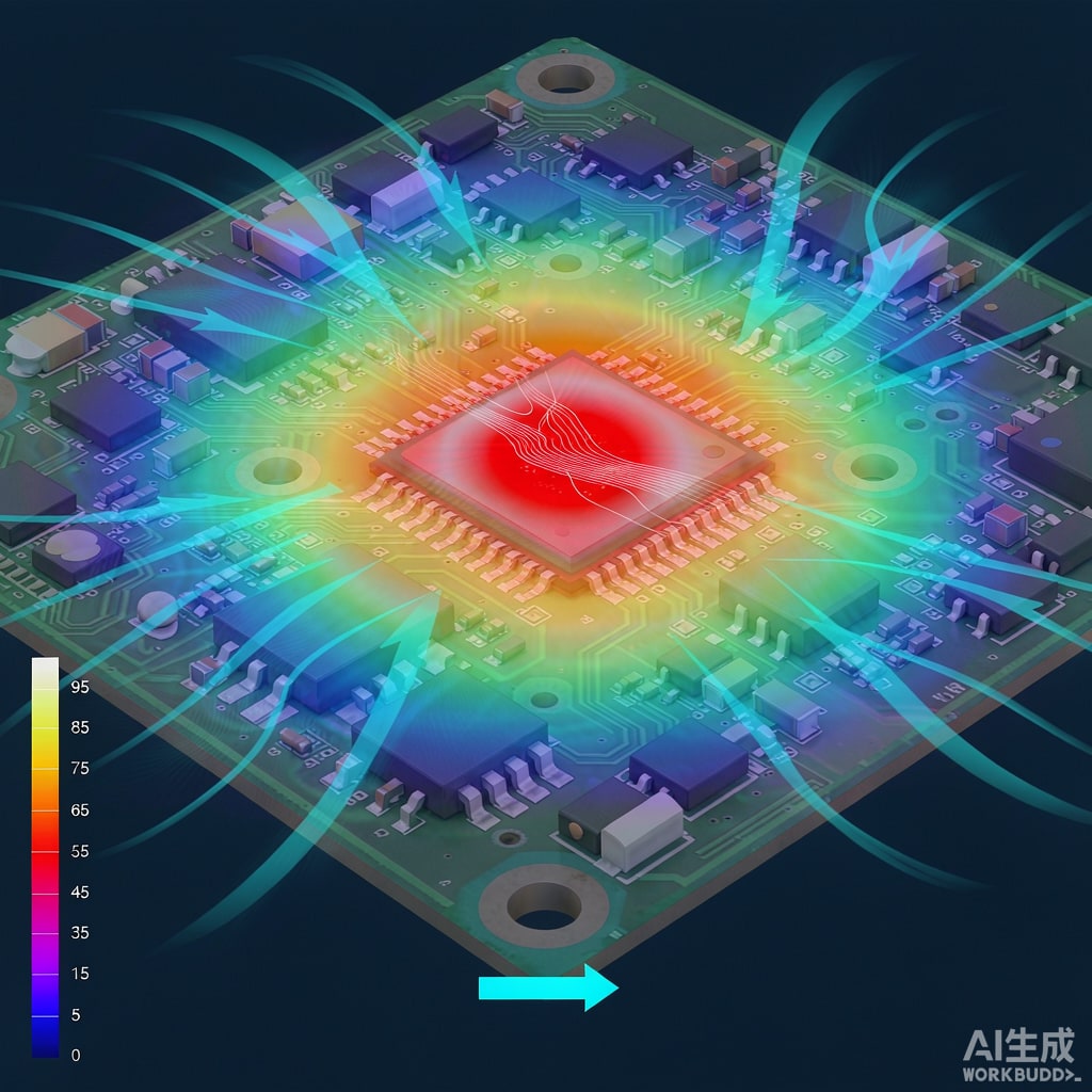
Most thermal simulation projects do not fail because the solver was wrong. They fail because the model described a board that does not exist: copper fractions averaged into a uniform block, a boundary condition picked from a defaults menu, and no validation run against a thermocouple. The result is a colorful picture that gets filed away and never used for a decision.
This is a practical workflow for board-level thermal simulation, aimed at engineers who need a defensible number rather than a beautiful contour plot.
Step 1: Define the Question Before You Open the Tool
Thermal models are expensive, and the level of detail you need depends entirely on what you are trying to learn. Decide which of these you are answering:
- Is the junction temperature under the limit? You need accurate component power, thermal path, and ambient. Copper distribution matters a lot.
- Where is the hot spot? You need accurate in-plane copper geometry and component placement, but rough absolute values may be acceptable.
- Will a design change help? You need a model that is sensitive to the change — which usually means higher fidelity in the region you are changing, not everywhere.
- Which of two enclosure layouts is better? This is a system-level airflow question, and the board may be representable as a block with effective conductivity.
A model built to answer the wrong question, however well converged, has no value. Write the question down before you start.
Step 2: Simplify With Intent
Copper Representation
Copper is the dominant heat spreading path on almost every board, and how you represent it decides the answer. Three options, in increasing fidelity:
- Uniform effective conductivity. Assign the laminate a single anisotropic conductivity derived from copper fraction. Fast, and adequate for system-level airflow studies. Dangerous for hot-spot prediction, because it smears the very gradients you are trying to find.
- Per-layer orthotropic conductivity. Model each layer with its own in-plane and through-plane conductivity based on the copper pattern. Modest effort, much better in-plane spreading fidelity.
- Explicit copper geometry. Draw the polygons, or import them from the layout database. Highest fidelity, highest meshing cost. Reserve it for the region around the hot component.
A good compromise, and the one worth defaulting to: explicit copper in a window around each significant heat source, orthotropic layers elsewhere, and a mesh transition between them.
Component Representation
- Detailed packages for the handful of components that dominate the thermal budget. Include the die, the die attach, the lead frame or substrate, the mold compound, and the solder joints.
- Two-resistor or Delphi-style compact models for everything else that dissipates meaningful power. These are available from most major semiconductor vendors and capture the junction-to-case and junction-to-board split without the meshing cost of a full package.
- Simple blocks with assigned power for the many small components that collectively warm the board but are not individually critical.
Vias
Thermal via arrays are often the single most important feature in the model and the easiest to get wrong. A 0.3 mm via on a 0.6 mm pitch with 25 micron copper plating has an effective through-plane conductivity far above the surrounding laminate, but treating the via field as a solid copper column overestimates it badly. Model the array as a region with an anisotropic conductivity computed from the via fill fraction, or model a representative subset explicitly and apply a symmetry boundary.
Step 3: Boundary Conditions Are the Whole Ballgame
This is where most models lose contact with reality.
Convection
A fixed convective coefficient is a guess, and the guess is usually a poor one, because natural convection coefficients vary strongly with orientation, temperature difference, and nearby surfaces. Options:
- For sealed enclosures or boards in still air, use a coupled CFD solve of the surrounding air rather than a fixed coefficient. The extra cost buys you the actual flow field, and with it the actual coefficients.
- For forced-air systems, model the enclosure and the fan curve. A fixed velocity inlet with a fixed outlet pressure is a reasonable simplification if the board does not significantly obstruct flow.
- If you must use a coefficient, derive it from a correlation appropriate to the geometry and orientation, and document the derivation. Do not accept a tool default.
Radiation
Radiation is routinely omitted and is often significant in still air. For a board with a high-emissivity soldermask in an enclosure, radiation can carry 20 to 40 percent of the heat at moderate temperature differences. Enable it with correct view factors and surface emissivity, or justify omitting it with a calculation.
Contact Resistance
Every mechanical interface in the model is a thermal resistance you must supply: TIM between a heat sink and a package, thermal pad between a package and a chassis, bolted joints, and the air gap between a board and a mounting boss. These interface resistances frequently exceed the resistance of the solid parts of the path. A model that omits them will predict a junction temperature that is optimistic by tens of degrees.
Step 4: Mesh Where It Matters
Mesh convergence is not a global exercise. Refine until the quantity you care about — usually a specific junction temperature — stops changing by more than a target percentage, for example 2 percent, between successive refinements. Two practical rules:
- Resolve the thermal boundary layer. If you are solving the fluid, the first cell height must be appropriate to the flow regime, and you need enough cells through the boundary layer to capture the gradient.
- Refine around sources and constrictions. The thermal resistance of a small die attach or a sparse via field lives entirely in the mesh resolution there.
Step 5: Validate, Always
An unvalidated model is an opinion with a color scale. Build a thermal test board or instrument the first prototype, and compare:
- Junction temperature via a thermal diode or the package’s built-in sense element, at a known power
- Board surface temperature at several points, via thermocouples or an IR camera
- Ambient conditions, recorded at the same time, including any radiating surfaces nearby
If the model is within a few degrees, calibrate the uncertain interface resistances against the measurement and note them for future models. If it is off by more than about 15 percent, find out why before you trust the model for a decision. The usual culprits, in order: missing interface resistance, wrong copper representation, and a boundary condition that does not match the test setup.
Practical Shortcuts Worth Knowing
- Board thermal conductivity is anisotropic. In-plane conductivity for an FR-4 board with typical copper is often ten to a hundred times the through-plane value. Getting this axis assignment wrong in the tool reverses the physics.
- Solder joints are not negligible. For a QFN with a thermal pad, the solder layer under the pad is a meaningful part of the junction-to-board path.
- Transient vs steady state. For pulsed loads, a steady-state model with average power will substantially overestimate temperature rise. Run transient analysis with the actual duty cycle.
- Keep a model library. Validated package models and calibrated interface resistances are reusable assets. Rebuilding them for every project is the most common waste of simulation time.
Making the Output Useful
Finish with a short thermal budget table listing each significant path — junction to case, case to heat sink, heat sink to ambient — with the resistance and the resulting temperature drop, alongside the validated total. That table is what the design team can act on, and what lets someone else check your work. A contour plot is a supporting exhibit, not a deliverable.
Get the model close to reality, validate it once, and reuse the validated pieces. Simulation then becomes what it should be: a way to test design options in an afternoon instead of a prototyping cycle.