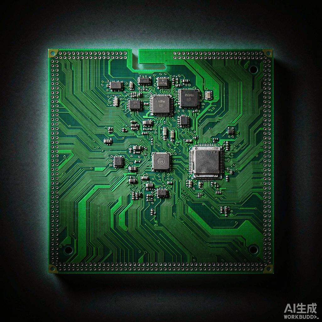
The Far-Field Problem at the Board Edge
When a high-speed digital signal traces out to a PCB edge without a controlled-impedance termination, the field pattern behaves like a slot ante
a. The edge becomes a radiating aperture, and common-mode current on the reference plane couples into free space. In Ethernet switches, USB 3.2 hubs, and HDMI 2.1 repeaters operating between 5 and 12 GHz, this edge radiation is the dominant source of EN 55032 Class B radiated emissions, often 6 to 12 dB above the regulatory limit even when every other layout guideline has been followed.
At TechMart SE we work with our industrial controller and networking OEM customers to apply two complementary edge treatments. Both are inexpensive, fully compatible with standard PCB fabrication, and together bring a marginal radiation problem back inside the regulatory envelope.
Edge Stitching: A Ground Via Fence Around the Board
Edge stitching is a row of plated-through-hole vias co
ecting all reference planes along the PCB perimeter. The vias are placed at a pitch of lambda-over-20 or tighter, where lambda is the wavelength of the highest harmonic of interest. At 10 Gbps NRZ the fifth harmonic is 25 GHz, for which lambda is 12 mm in FR-4, giving a lambda-over-20 pitch of 0.6 mm. We typically recommend a stitching pitch of 0.5 mm or 1.0 mm depending on fabrication capability, with the via diameter at 0.25 to 0.3 mm and the pad diameter at 0.45 to 0.55 mm.
The fence works by converting the open edge into a chain of small waveguides-below-cutoff structures. Each via pair imposes a local boundary condition that prevents the fringing field from building across a complete wavelength along the edge. Practical measurements from a 100 mm by 80 mm 4-layer board show that adding a single row of stitching at 1.0 mm pitch reduces 5 to 12 GHz radiated emissions by 8 to 14 dB compared with no stitching.
Edge Plating: A Continuous Metallurgical Edge
Edge plating takes the concept one step further. Instead of discrete vias, the entire PCB edge is metallized using a special plating process in which the routed edge is brought into contact with electroless copper plus electrolytic plating baths. The result is a 5 to 25 micrometre copper skin on the edge, perfectly continuous. Edge-plated vias on the perimeter can then be soldered directly to the edge plating, producing a 360-degree shield around the board.
From a fabricator perspective, edge plating requires a sacrificial routing edge and plated-edge masking tape to keep non-edge copper surfaces out of the bath. The cost adder is modest, usually 8 to 14 percent per panel, but for high-volume consumer products it delivers another 6 to 10 dB of attenuation above the stitching-row baseline. Many Apple-class devices combine edge stitching plus edge plating plus a single-piece sheet-metal shield can for total enclosure SE above 50 dB at 6 GHz.
Why the Pitch Must Follow a Wavelength Rule
Some layout guides recommend a 5 mm or 10 mm stitching pitch based on mechanical rules of thumb, but this is ineffective above 3 GHz. A 10 mm pitch corresponds to lambda-over-12 at 2.5 GHz and lambda-over-3 at 10 GHz; the latter violates the waveguide-below-cutoff condition and the fence becomes transparent at the frequencies of interest. The lambda-over-20 rule is conservative and works at the cost of more vias; lambda-over-10 is acceptable for cost-sensitive layouts and still gives 5 to 7 dB of attenuation.
Stackup and Stitching Symmetry
For the perimeter fence to function correctly, stitching vias must co
ect every reference plane in the stack. In a 6-layer board with L2 ground and L5 ground, the same via should stitch both layers simultaneously, which is automatic in a standard through-hole but may not be true for partial-depth back-drilled vias. Symmetry also matters: if stitching via row A is on the top edge but the corresponding row B on the bottom edge is missing or offset, the structure becomes an asymmetric slot. Match all four edges.
Verification in Lab and Production
Verify edge stitching performance with a 3-meter or 10-meter semi-anechoic chamber scan per EN 55032, plus a current probe loop measurement at the PCB edge to confirm common-mode current is suppressed by 10 dB or more. Production QA can use a time-domain reflectometer to confirm via continuity and a stitch-to-stitch loop inductance measurement that should not exceed 1 nH per 5 mm of perimeter stitching row.



