Every SMT power design eventually runs into the same question: how hot is too hot? Datasheets specify absolute maximum junction temperatures of 125 °C or 150 °C, but designing a power supply or LED driver to run its components at those limits is a guaranteed reliability problem. Junction temperature budgeting turns vague worry into a number you can verify, and derating rules tell you how far below the maximum you should actually operate.
Why TJ Max Is Not a Design Target
The absolute maximum junction temperature is the point at which the semiconductor die suffers immediate damage or parametric destruction. Long before that, reliability mechanisms accelerate: electromigration in metal interco
ects roughly doubles in rate for every 10 °C increase, solder joint fatigue life falls exponentially with cycling amplitude, and electrolytic capacitor lifetime halves for every 10 °C rise in core temperature. A component that survives at 125 °C junction will see its field failure rate multiply compared to one ru
ing at 90 to 105 °C. Mature design organizations therefore adopt a derated operating target, typically 80 to 110 °C depending on application class.
Building the Budget
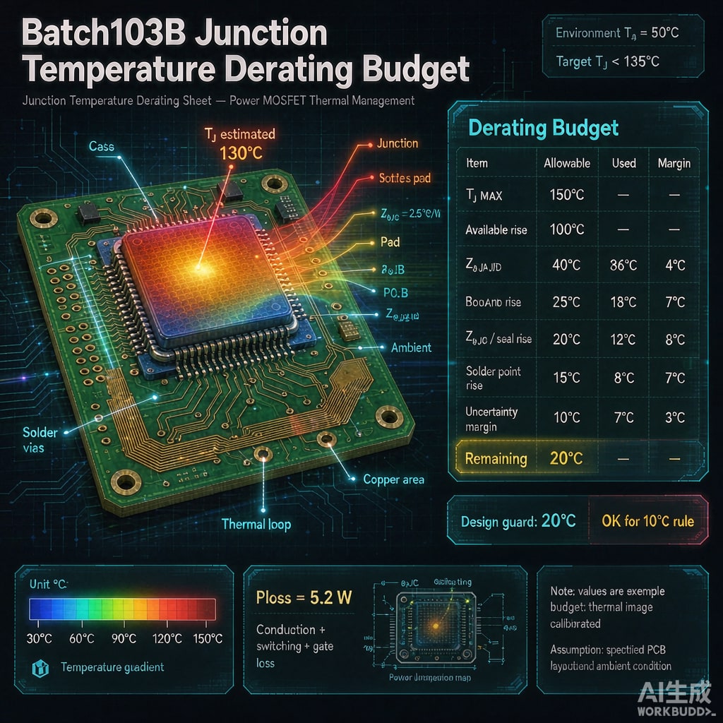
A junction temperature budget is a simple stack of temperature rises added to the worst-case ambient. For each power component, work through four steps:
Step 1: Fix the Ambient Assumption
Use the real worst case, not the datasheet standard. For a fanless adapter in a sealed enclosure in a tropical market, 50 to 60 °C inside the case is realistic. For industrial control cabinets, 55 °C is a common design point. Documenting this number and getting agreement before layout prevents late-stage redesign.
Step 2: Sum the Thermal Resistances
The junction-to-ambient path is a series stack: die to package (RθJC), package to board via solder and thermal vias (RθCS plus contact resistance), board spreading (copper planes), and board to air (RθSA). Use the package-specific RθJC from the datasheet, but compute the board-side terms yourself; datasheet RθJA values assume JEDEC still-air test boards that rarely match your layout. A QFN with a 3 mm × 3 mm exposed pad on a four-layer board with a 25 mm copper pour typically achieves 35 to 45 °C/W board-side; the same part on a two-layer board may exceed 90 °C/W.
Step 3: Compute the Rise
Multiply total power dissipation by the stack resistance. Be honest about dissipation: use conduction plus switching losses at the actual switching frequency and load profile, not the peak efficiency point. For pulsed loads, use transient thermal impedance curves rather than the steady-state value; a 10 ms pulse can see an effective impedance one-tenth of the DC figure.
Step 4: Compare Against the Derated Limit
If the computed junction exceeds the derating target, you have three levers in order of preference: reduce power loss (better topology, lower RDS(on), softer switching), improve the heat path (more copper, thermal vias, a heat sink), or reduce the ambient (ventilation). Attempting to argue the derating down is the weakest option.
Common Derating Policies
- Consumer electronics: 105 °C junction for silicon, 110 to 120 °C for power MOSFETs in short excursions, with continuous operation typically below 95 °C.
- Industrial and telecom: 90 to 100 °C continuous, matching the expected 10 to 20 year service life.
- Automotive: suppliers commonly require junctions at or below 110 °C continuous with peaks to 125 °C, aligned with AEC-Q100 grade expectations.
- LED lighting: the LED junction, the electrolytic capacitors, and the driver ICs all get budgets; the capacitors usually impose the tightest limit despite lower TJ ratings.
Whatever policy you adopt, write it into the design review checklist so the budget is actually checked, not just assumed.
Validating the Numbers
Budgets built on paper must be confirmed on hardware. Three techniques cover most cases:
- Case temperature extrapolation: measure the package top or exposed pad with a fine-gauge thermocouple, then back-calculate the junction using TJ = TC + P × RθJC. Accuracy depends on the thermocouple being flush to the surface and insulated from airflow.
- Temperature-sensitive parameter (TSP) measurement: the forward voltage of a diode or the on-resistance cha
el of a MOSFET varies predictably with temperature; powering one junction while sensing another gives a direct junction reading in packaged devices.
- IR thermography: useful for relative mapping and finding unexpected hot spots, but emissivity differences across a mixed PCB make absolute readings unreliable without calibration targets.
Test at maximum ambient, maximum load, and minimum airflow simultaneously. Thermal images at 25 °C room temperature routinely hide violations that appear at 45 °C.
Conclusion
Junction temperature budgeting is not exotic analysis; it is disciplined arithmetic plus honest assumptions about ambient, losses, and thermal resistance. Choose a derating policy matched to the product’s service life, build the budget early enough to influence the layout, and verify with real measurements at true worst-case conditions. Designs that respect these rules ship without thermal surprises; designs that treat TJ max as a target come back as warranty claims.