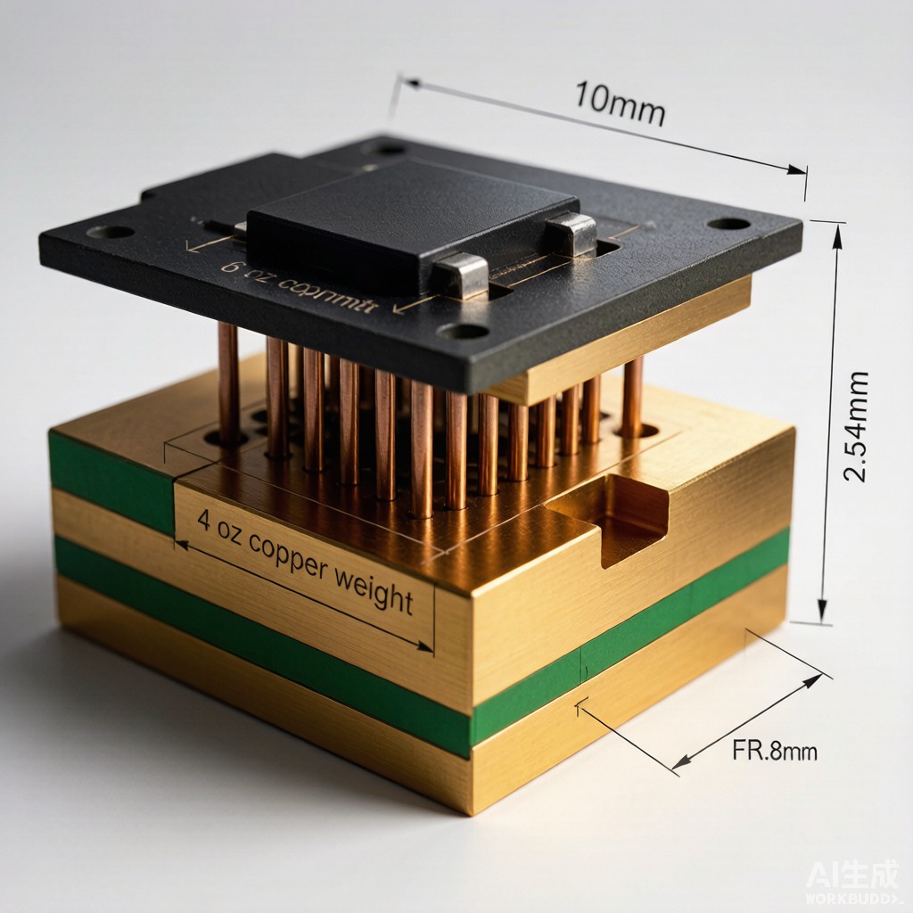
The migration of power conversion systems from discrete through-hole components to SMT-assembled power modules has intensified thermal management requirements beyond the capability of standard 1-2 oz copper PCB substrates. Heavy copper PCB technology, defined as finished copper weight of 3 oz/ft² (105 µm) to 20 oz/ft² (700 µm) on external layers and corresponding thicknesses on i
er layers, provides the necessary current-carrying capacity and thermal spreading for high-power SMT power modules. In Southeast Asian deployment where ambient temperatures routinely reach 35-40°C and humidity exceeds 80% RH, the thermal derating of standard PCB materials often forces designers to over-specify module ratings or accept reduced reliability margins. This article examines the engineering principles of heavy copper PCB thermal management for SMT power module assembly.
Heavy Copper PCB Construction and Material Stack-Up
Copper Weight Classification
The IPC-6012 standard classifies copper weight by finished foil thickness measured in ounces per square foot:
| Class | Cu Weight (oz/ft²) | Thickness (µm) | Typical Application |
|---|---|---|---|
| Standard | 0.5-2 | 17-70 | Signal layer, low-power SMT |
| Heavy | 3-6 | 105-210 | Power module substrate, 50-200A |
| Extreme Heavy | 8-20 | 280-700 | EV inverter, 400-800A busbar |
Substrate Material Selection
Standard FR-4 with Tg 130-150°C remains usable for heavy copper applications where junction temperature stays below 125°C, but for high-power modules with junction temperatures reaching 150-175°C, the substrate must upgrade to:
-
<l
- High-Tg FR-4 (Tg 170-180°C): Modified epoxy with dicyclopentadiene (DCPD) backbone. CTE z-axis reduced to 60-80 ppm/°C below Tg vs 250-350 ppm/°C for standard FR-4 above Tg.</l
- <l
- Modified epoxy (Tg 180-200°C): Phenolic-cured multifunctional epoxy. Suitable for 150°C continuous operation.</l
- <l
- BT epoxy / cyanate ester: Tg 220-260°C, low Dk/Df for high-frequency power modules.</l
- <l
- Thermally conductive prepreg: Alumina or boron nitride filled prepreg with thermal conductivity 1.5-3.0 W/m·K (vs 0.25-0.35 W/m·K for standard FR-4).</l
Thermal Management Architecture
Copper Plane Heat Spreading
Copper in-plane thermal conductivity of 385-400 W/m·K (C11000) creates an exceptional heat-spreading layer. The thermal resistance from a 10mm × 10mm heat source to a 50mm × 50mm spreader plane on 3 oz copper (105 µm) is approximately 0.18 K/W. Doubling the copper weight to 6 oz reduces this to 0.09 K/W, a 50% reduction with no dielectric change. However, the spreading benefit plateaus beyond 6 oz because lateral conduction becomes limited by the heat source footprint rather than plane thickness.
Thermal Via Array Engineering
Thermal vias transfer heat from SMT power component pads to i
er copper planes or bottom-side heat sinks. Key design parameters:
-
<l
- Via diameter: 0.20-0.30 mm drill (0.40-0.55 mm finished) typical; smaller vias reduce solder wicking risk but increase drill cost.</l
- <l
- Via pitch: 0.8-1.2 mm center-to-center, creating 6-12 vias per cm² density.</l
- <l
- Plating thickness: 25-35 µm copper plating per IPC-6012 Class 3 for high-current applications.</l
- <l
- Via filling: Conductive epoxy (silver-filled) or copper-filled via-in-pad eliminates solder voiding and improves thermal transfer by 20-30% versus unfilled vias.</l
- <l
- Copper coin / heat slug: Direct bonded copper (DBC) or pressed-in copper coin embedded in PCB cavity provides 2-3 W/m·K effective through-plane conductivity, matching IMS substrates at lower cost.</l
Thermal Via Array Calculation
For a 100W SMT power module dissipating 60W with junction-to-case thermal resistance target of 0.5 K/W, the required via thermal resistance from top copper to bottom heat sink is:
Rθ_via_array = (T_junction – T_sink) / Q – Rθ_jc – Rθ_sink = 1.0 – 0.3 – 0.2 = 0.5 K/W
With 2.0mm thick FR-4 (Rθ_dielectric 0.057 K/W per layer of standard prepreg), 0.3mm finished via diameter, 1.0mm pitch, and 1.5mm copper plating, each via contributes approximately 35 K/W individually, or 1.1 K/W in parallel for 32 vias. The required via count for 0.5 K/W total is approximately 70 vias under the heat source footprint.
SMT Assembly Considerations for Heavy Copper
Thermal Mass Profiling
Heavy copper PCB presents significant thermal mass challenges during reflow soldering. A 6-layer 4 oz PCB weighs 1.8-2.2 kg/m² versus 0.8-1.0 kg/m² for standard 1 oz construction. The thermal time constant at the center of the board extends to 180-240 seconds versus 90-120 seconds for standard PCBs, requiring:
-
<l
- Extended preheat zone (Zone 1-2): 120-180 seconds at 150-180°C to equalize temperature across the heavy copper planes.</l
- <l
- Higher peak temperature: 245-250°C peak for SAC305 lead-free solder (vs 240-245°C for standard PCB) to overcome thermal mass.</l
- <l
- Total time above liquidus (TAL): 60-90 seconds to ensure complete solder wetting on all component pads including those over heavy copper planes.</l
- <l
- Cooling rate: Controlled cooling at 2-3°C/sec to prevent IMC growth while avoiding warpage from differential copper CTE.</l
CTE Mismatch and Solder Joint Reliability
The CTE mismatch between silicon die (2.6 ppm/°C), copper lead frame (17 ppm/°C), and PCB substrate (14-17 ppm/°C in-plane) creates cyclic stress at the solder interface. For a power cycling test profile of -40°C to +150°C with 1,000 cycles, the accumulated plastic strain in the solder joint is approximately:
γ = (CTE_die – CTE_board) × ΔT × L / h = (2.6 – 14) × 190 × 5mm / 0.1mm = 0.108 (10.8% strain)
This exceeds the SAC305 fatigue limit of 5-7% strain, requiring mitigation through underfill (epoxy capillary underfill, 70-80% fillet coverage reduces strain by 40-60%) or lead-frame design (down-set geometry, copper clip bonding).
Reliability Verification and Acceptance
Thermal Cycling Qualification
Heavy copper PCB modules for automotive and industrial applications require thermal cycling qualification per:
-
<l
- AEC-Q100/Q104: -40°C to +125°C, 1,000 cycles for Grade 1, 2,000 cycles for Grade 0.</l
- <l
- IPC-9701: Thermal cycling profile 0°C to +100°C with 5-10 minute dwell, monitoring resistance change less than 10% over 6,000 cycles.</l
- <l
- Power cycling: Per MIL-STD-750 Method 2037, junction temperature swing ΔTj 100°C with 5-minute on/off cycle.</l
Failure Mode Analysis
Common heavy copper PCB failure modes include:
-
<l
- I
er layer delamination:
Z-axis expansion of FR-4 above Tg separates copper foil from substrate. Mitigation: use high-Tg material and control peak temperature during reflow.</l - <l
- Barrel cracking: Differential CTE between copper plating and PCB material fractures via barrel in thermal cycling. Mitigation: filled vias with compliant i
er fill material.</l
- <l
- Solder joint fatigue: Creep and isothermal fatigue of SAC305 at elevated temperature. Mitigation: underfill or lead-free silver-containing solder (SAC105, I
olot).</l
- <l
- Electromigration: High current density (10⁴-10⁵ A/cm²) at 150°C accelerates copper ion migration. Mitigation: keep current density below 500 A/cm² at maximum operating temperature.</l
Conclusion
Heavy copper PCB technology enables SMT power module assembly for applications exceeding 50A continuous current and 100W power dissipation, with thermal resistance and current capacity 5-10x higher than standard 1-2 oz PCB construction. Successful implementation requires careful coordination of substrate material selection (high-Tg or thermally conductive prepreg), thermal via array design (filled vias under power components), reflow profile engineering (extended preheat and peak temperature), and reliability qualification (thermal cycling, power cycling, and failure mode analysis). For tropical Southeast Asian deployment where ambient temperatures compound cooling challenges, the heavy copper PCB approach provides a robust substrate for next-generation power electronics manufacturing.



