Heat sink base thickness is one of the most frequently guessed parameters in thermal design. Too thin and the base fails to spread heat from a small die, leaving the outer fins starved. Too thick and you pay in mass, cost, and starting conduction height that could have been fins. This article gives a working method for optimizing base thickness, with rules of thumb that hold up in practice.
Why Base Thickness Matters: Spreading Resistance
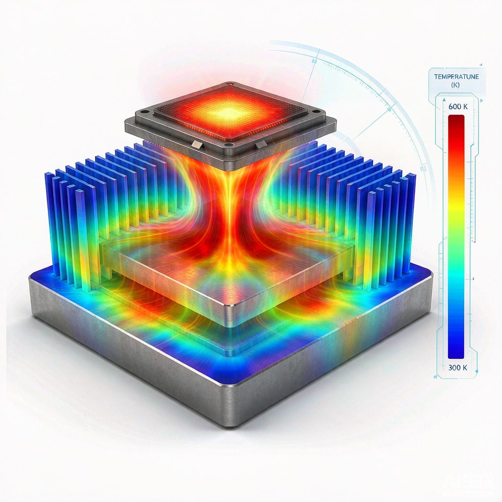
When a heat source smaller than the heat sink footprint dumps heat into the base, heat must spread laterally before reaching the fin field. The thermal resistance of this spreading process adds to the one-dimensional conduction resistance through the base. Spreading resistance depends on the source-to-base area ratio, base thermal conductivity, base thickness, and the TIM/attachment stack. For a 15×15 mm die on a 100×100 mm aluminum heat sink, spreading resistance can dominate — sometimes exceeding the fin resistance itself if the base is under-thicknessed.
The U-Curve
Plot total thermal resistance against base thickness and you get a U-shaped curve. It falls steeply at small thicknesses (spreading improves quickly), reaches a broad minimum, then rises slowly (pure conduction through the extra copper). The optimum is usually broad: anywhere within ±30% of the optimum thickness changes performance by only a few percent. That is good news — you do not need precision, just the right region.
Rules of Thumb by Source Size and Material
Copper Bases
For copper (k ≈ 390 W/m·K), a practical optimum base thickness is roughly 1.5–2.5× the square root of the source area in mm. A 20×20 mm source lands at 6–10 mm; a 10×10 mm source at 3–5 mm. Because copper spreads well, going thicker yields little and adds serious mass (copper is 3.3× denser than aluminum).
Aluminum Bases
For extruded aluminum (k ≈ 180–200 W/m·K for 6xxx alloys), the same rule gives about 2–4× the source square root, and real-world extrusions often cluster at 4–10 mm regardless, because extrusion tooling and flatness set floors. When the calculated optimum exceeds what an extrusion can practically offer, consider a bonded or skived copper base insert under the die region — a hybrid that recovers most spreading performance at a fraction of an all-copper part’s weight.
Multiple Sources
With several hot components on one base, the effective source area is not the sum — it is governed by the largest single source and the spacing between them. Sources closer than roughly 3× base thickness to each other partially share spreading benefits; spaced-apart sources each need their own spreading allowance.
The Quantitative Shortcut
For those who want a number without CFD, the classic spreading resistance approximation (Lee/Song style closed-form solutions, implemented in most vendor spreadsheets) needs five inputs: source size, base size, base thickness, base conductivity, and effective contact conductance under the source. Five minutes with the vendor calculator beats a guess. Sanity checks: if the source is more than about 40% of the base linear dimension, spreading resistance is minor — choose thickness for structural rigidity and fin attachment, not spreading. If the source is under 10% of the base, spreading dominates and thin bases hurt badly.
Weight, Mounting, and Flatness Constraints
Weight Budget
Every millimeter of extra copper base on a 100×100 mm sink adds about 89 g. In portable, airborne, and wall-mounted electronics, base thickness is often the first thing to trim when a mass target is missed. Aluminum’s 3.3× density advantage means an aluminum base can be ~50% thicker for the same mass — sometimes the better spread-per-gram choice when conductivity is adequate.
Flatness and Mounting Pressure
Thin bases bow under clip or screw mounting pressure, distorting the TIM interface and lifting fin-field tolerances. As a rule, keep base thickness at least 3–4 mm when using four-point spring clips on large bases, or spec a thicker local boss under the die. Base flatness under the source should be held to 50 µm or better for grease-type TIMs; a too-thin base makes that specification expensive to hold.
Cost Trade-Offs
Thicker extrusion costs little in tooling but more in material and machining time. Copper bases multiply raw material cost and often force a two-part construction (copper base + aluminum fins) with brazing or soldering. Before upsizing the base, compare against alternatives that attack spreading directly: vapor chambers (excellent for very small hot spots, higher cost), heat pipes embedded in the base (good for transporting heat away from the source region), or simply shrinking the base footprint to reduce the spreading ratio. Frequently the cheapest fix is a denser fin field under the die — concentrating fins where heat actually is — rather than more base metal.
A Worked Example
Consider a 20×20 mm GaN power module dissipating 120 W onto a 120×90 mm sink. Rule of thumb for copper: 1.5–2.5 × √400 = 6–10 mm base. Vendor calculator at 8 mm copper shows spreading resistance ≈ 0.05 K/W; at 4 mm it rises to ≈ 0.11 K/W — a 7°C junction penalty at 120 W. In aluminum, matching that spreading needs ~15 mm and 2.1 kg; the copper base at 8 mm weighs 0.82 kg. Hybrid copper-base/aluminum-fin construction lands between on both axes. This is the shape of the decision: quantify spreading, price the mass, and pick the region — not the millimeter.