Two Materials, Two Different Jobs
Most thermal discussions on SMT boards conflate two separate functions: moving heat away from a die or power pad, and moving heat sideways across a board. Copper does both competently. Graphite does the second one exceptionally and the first one badly.
Pyrolytic graphite sheet, usually supplied at 0.025 to 0.1 mm, reaches 1,500 to 1,950 W/m·K in plane while conducting only 5 to 15 W/m·K through its thickness. Copper C11000 sits at 390 W/m·K in every direction. That anisotropy is not a defect to be worked around; it is the entire point of the material, and it dictates where it belongs.
The Numbers That Actually Drive Selection
| Property | Pyrolytic graphite sheet | A
ealed graphite sheet |
Copper C11000 | Aluminum 6061 |
|---|---|---|---|---|
| In-plane conductivity (W/m·K) | 1,500–1,950 | 300–500 | 390 | 167 |
| Through-plane (W/m·K) | 5–15 | 3–6 | 390 | 167 |
| Density (g/cm³) | 1.9–2.2 | 1.0–1.6 | 8.94 | 2.70 |
| In-plane CTE (ppm/K) | −1 to +1 | −1 to +1 | 17 | 23 |
| Electrical conductivity | Conductive | Conductive | Conductive | Conductive |
| Solderable | No | No | Yes | With plating |
Two rows deserve attention. Density means a 0.1 mm graphite spreader weighs about 0.2 g per 10 cm², against 0.9 g for the same area in 0.1 mm copper. In a handheld device with three spreaders, that is a couple of grams, which is real battery life. The negative in-plane CTE means graphite contracts slightly when heated, opposite to solder and FR-4, which is the root of most delamination complaints.
Where Graphite Wins Clearly
Hot spot spreading under large BGAs and power modules
Spreading resistance scales inversely with conductivity times thickness. For a 10 × 10 mm heat source on a 40 × 40 mm spreader, a 0.1 mm graphite sheet at 1,700 W/m·K outperforms 0.5 mm copper while using a fifth of the volume. Where a design is limited by a hot spot rather than by total heat, graphite is the cheaper answer than thickening the copper plane.
Z-height constrained products
Smartphones, wearables, and camera modules rarely have 0.5 mm to spare. A 0.05 mm graphite sheet laminated to a shield can or a display backplate can be the only spreading option that fits.
Isolating two thermal domains
Because through-plane conductivity is poor, graphite is an accidental thermal insulator across its thickness. That is useful when you need to spread heat within a plane but avoid dumping it into a temperature-sensitive component directly beneath.
Where Copper Still Wins
Any vertical heat path
If the heat must travel through the spreader into a heat sink, a chassis, or a thermal pad, graphite adds a bottleneck. A 0.1 mm sheet with kz of 10 W/m·K contributes roughly 0.1 K·cm²/W of resistance, which sounds small until you compare it with a good thermal interface at 0.3 to 0.5 K·cm²/W and realize the spreader is now 20% of the stack.
Grounding, shielding, and current carrying
Copper spreaders double as ground planes and EMI reference surfaces. Graphite is electrically conductive too, which sounds equivalent until you try to solder to it, plate it, or bolt a ground strap to it reliably. It ca
ot be soldered with conventional paste and it ca
ot be reflowed as part of the board stack.
Mechanical robustness
Graphite sheet flakes and sheds. Under vibration, at board edges, or where a co
ector rubs, it produces conductive particles that migrate into fine-pitch areas. Copper does not.
Attachment Methods and the Resistance They Add
Pressure-sensitive adhesive
The standard graphite PSA is an acrylic loaded with ceramic filler at 0.2 to 0.5 W/m·K, applied at 20 to 50 µm. That adhesive layer often dominates the whole thermal path. For a pressure-only contact you can expect 1 to 3 K·cm²/W; a well-bonded adhesive joint gets to 0.3 to 1.0 K·cm²/W.
Thermally conductive double-sided tape vs dispensed adhesive
Tape is fast and reworkable but leaves 30 to 50% void fraction if the surface is not flat. Dispensed alumina-filled epoxy gives better wetting and lower resistance, at the cost of being permanent.
Mechanical clamping
Clamping works for thick graphite (>0.5 mm) but crushing thin sheet under a screw boss shears it. Use a compliant pad between the clamp and the graphite, and never clamp within 1 mm of a cut edge.
Electrical isolation is mandatory
Graphite touching a live pad or a component lead is a short. Every graphite spreader needs either an insulating PSA on both faces or a dielectric film (polyimide tape, 25 µm) at the boundary. Designers forget this roughly once per project, and the resulting field failure is intermittent and expensive to diagnose.
Failure Modes Worth Designing Against
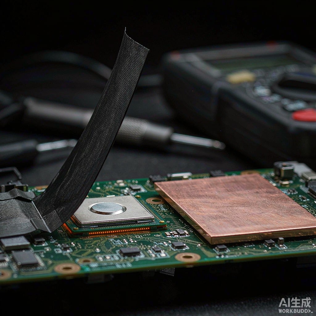
- Edge flake shedding. Seal cut edges with 10 to 20 µm polyimide tape, or specify die-cut parts with encapsulated edges from the converter. Never hand-cut graphite in a production area.
- Delamination under thermal cycling. The CTE mismatch concentrates shear at the perimeter. Cycle test −40 to +125°C for 500 cycles and inspect edges; a spreader that lifts at one corner has already lost most of its contact area.
- Compression set in the adhesive. Thin PSA creeps under sustained pressure at elevated temperature. Avoid designs where the only retention is adhesive plus a spring force.
- Moisture ingress. Graphite is porous at the edges and can wick flux and cleaning solvents, which later outgas inside a sealed enclosure.
Hybrid Stacks: The Practical Compromise
The best-performing and most manufacturable answer is usually a laminated hybrid: a 0.2 to 0.4 mm copper plate for the vertical path and mechanical anchoring, with a 0.05 mm graphite sheet bonded on top to spread laterally before the heat reaches the copper. The graphite handles spreading resistance, the copper handles transport and grounding, and the graphite can be die-cut to avoid keep-out zones entirely.
Selection Checklist
- Is the limiting resistance spreading (hot spot) or transport (total heat)? Spreading favors graphite; transport favors copper.
- Does the heat path turn vertical anywhere? If yes, copper or a hybrid.
- Is there realistic Z-height available? Under 0.3 mm, graphite is usually the only option.
- Is the surface already carrying ground or current? Copper avoids a second part.
- Can the assembly tolerate conductive particles? If not, seal edges or choose copper.
- What does the interface actually measure, not what the datasheet claims? Verify with a laser flash or steady-state stack test on the finished assembly, not on the raw sheet.