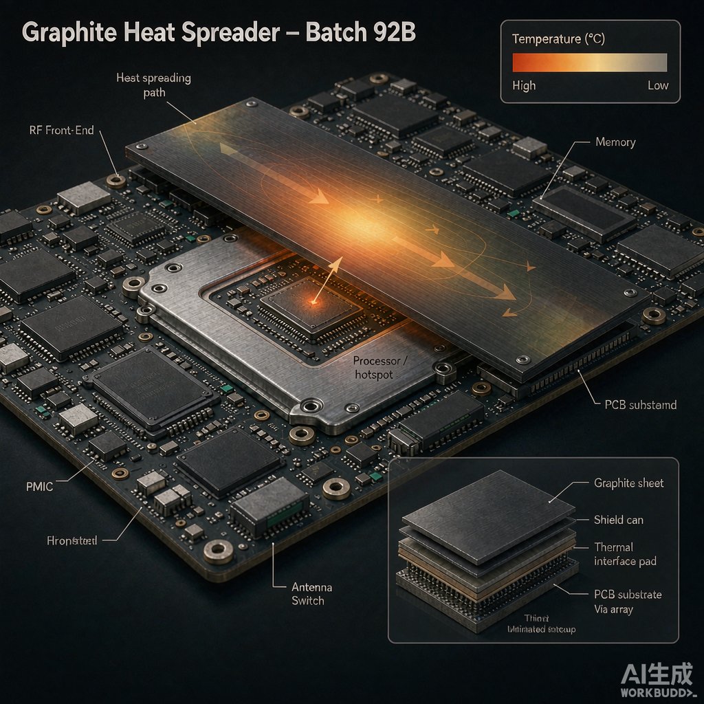
Smartphones, wearables, routers, and compact IoT gateways have no fans, no airflow, and less and less free volume, yet their SoCs and power management ICs routinely dissipate several watts. In these sealed products the dominant thermal problem is not removing heat to the air but spreading it away from a small hot spot into a larger structure. Synthetic graphite heat spreader sheets have become the default answer because they conduct heat laterally extremely well while staying thin, light, and flexible. This guide explains how they work, how to select thickness and grade, and how to integrate them on PCB assemblies and housings.
Why Lateral Heat Spreading Matters in Fanless Designs
A die that dissipates 3 W over a 10 by 10 mm footprint creates a steep local temperature rise on a bare PCB because FR-4 spreads heat poorly in-plane, around 0.3 to 0.9 W/m-K, and only modestly better through its thickness. The result is a concentrated hot spot: one spot approaches the thermal limit while the surrounding board stays cool and unused as a radiator. A heat spreader with high in-plane conductivity grabs heat from the hot spot and distributes it over ten to thirty times the area, lowering the peak temperature and letting the whole enclosure participate in cooling. In sealed devices this spreading step routinely buys five to fifteen degrees C of hotspot relief, which is often the difference between throttling and full performance.
How Synthetic Graphite Works
Synthetic graphite sheet is made by carbonizing polyimide film and graphitizing it at very high temperature, aligning graphite crystals in the plane of the sheet. The result is strongly anisotropic: in-plane thermal conductivity from roughly 700 up to 1950 W/m-K depending on grade, against only 5 to 15 W/m-K through-plane. Density is low, about 1.7 to 2.1 g/cm3, and sheets as thin as 17 micrometers can be die-cut into almost any shape and laminated with adhesive and insulating layers.
Grade Selection: Thickness Versus Conductivity
- Standard grades (17 to 25 micrometers, 700 to 1000 W/m-K): the workhorse for phones and small modules where space above the board is minimal and the sheet must survive repeated bending.
- Enhanced grades (25 to 40 micrometers, 1000 to 1500 W/m-K): better spreading per pass for gaming devices, 5G radios, and camera modules with bigger heat sources.
- High grades (40 to 100 micrometers, 1500 to 1950 W/m-K): used as a single thick layer or stacked where a narrow bridge must carry heat from the board to a metal frame; stiffer and more fragile, so they are usually supported by laminates.
A useful sizing check is the in-plane conductance of the sheet, which is conductivity multiplied by thickness. A 25 micrometer sheet at 1000 W/m-K carries about 0.025 W per kelvin of in-plane temperature gradient per meter of width; doubling thickness or conductivity doubles that capacity. When the required lateral heat flow is known from simulation or measurement, this simple product tells you quickly whether one layer is enough or a stack is needed.
Balancing Spreading and Through-Plane Resistance
Because through-plane conductivity is low, graphite is not good at pushing heat into a cold wall by itself. Every interface adds contact resistance, and the sheet only helps if both ends are well coupled: one end bonded over the hot spot or shield can, the other end bonded over a large metal surface. Where heat must cross into a housing, designers combine a thin graphite sheet in-plane with a small thermal pad or gap filler through-plane, letting each material do what it does best.
Integrating Graphite Sheets on PCBs and Housings
Good integration is mostly about placement and insulation:
- Place the sheet over the die or shield can covering the hotspot, then extend it over as much adjacent cool area as space allows; spreading area matters more than elegance.
- Use electrically insulating laminates. Graphite is conductive; sheets that pass over exposed pads, ante
as, or component legs need a PET or PI insulating top and bottom layer, and edges must not short fine-pitch circuits.
- Bridge into the enclosure by wrapping the sheet around the board edge onto the mid-frame or metal back cover, converting the whole shell into a radiator.
- Respect bending limits. Thin sheets tolerate tight radii; thick high-conductivity sheets crack if folded sharply, so route them over gentle curves rather than 90-degree folds.
- Die-cut with clearances around co
ectors, buttons, and ante
a areas, and choose adhesive strength for the service temperature so the sheet does not peel during thermal cycling.
Graphite Versus Copper Foil Versus Thermal Pads
Copper foil spreads well too, around 390 W/m-K, and it conducts through-plane as well as in-plane. But to match a good graphite sheet laterally you need roughly four to six times the thickness, which means four to six times the weight, and thick copper work-hardens and transfers less neatly onto curved surfaces. Graphite delivers two to four times copper’s in-plane conductivity at a fraction of the thickness, which is why thin devices standardized on it. Thermal pads and gap fillers solve the opposite problem: they move heat vertically from chip to lid with good compliance, but they spread almost nothing laterally. High-performance stacked solutions therefore use all three: a gap filler to reach the shield, graphite to spread across it, and the housing as the final radiator.
Validation From Simulation to Thermal Imaging
Start with a transient thermal simulation or a simple spreading-resistance estimate to size the sheet, then verify on hardware. Infrared imaging through shield openings or on the housing surface shows how well the hot spot has been flattened; thermocouples on the die-adjacent surface and on the far end of the spreader reveal the in-plane gradient. Run the comparison at maximum sustained power, and repeat after power cycling to confirm that adhesives and laminates survive hundreds of thermal swings. A sheet that measured well on day one but lifted at its adhesive line after cycling will quietly surrender most of its benefit.
Conclusion
Graphite heat spreaders solve the defining thermal problem of sealed compact electronics: moving heat from a tiny die across a board that ca
ot spread it on its own. Selection is straightforward once you fix the hot spot, estimate the required lateral heat flow, and choose grade and thickness so the in-plane conductance covers it with margin. Combine the sheet with a through-plane interface material where heat must enter the housing, insulate it where it crosses live circuits, and validate with thermal imaging after power cycling. TechMartSe supports electronics manufacturers across Southeast Asia with thermal management components, including graphite heat spreader solutions, copper-based spreaders, and interface materials for PCB-level cooling designs.



