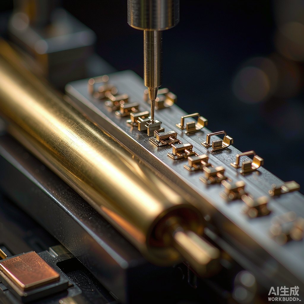
Why Gold Plating Matters at High Frequencies
As 5G, Wi-Fi 6E, and millimeter-wave radar push signal frequencies beyond 6 GHz, conductor surface behavior dominates performance. At these frequencies, current crowds within a shallow skin depth—often less than 1 µm for copper. A thin, stable, low-resistance surface layer becomes critical, which is why gold-plated copper strip is the material of choice for high-frequency SMT co
ectors, ante
a feeds, and RF test fixtures.
Skin Effect and Surface Resistance
Skin depth (δ) decreases with the square root of frequency. At 10 GHz, copper’s skin depth is approximately 0.66 µm. Any surface oxidation, contamination, or roughness increases effective resistance and introduces insertion loss. Gold offers:
- Immunity to oxidation: Gold does not form insulating oxide films, ensuring consistent contact resistance over years.
- Low electrical resistance: Bulk resistivity of gold (~2.4 µΩ·cm) is higher than copper, but at RF the effective resistance is dominated by surface condition, not bulk material.
- Excellent solderability and wire-bondability: Soft gold (99.9% pure) supports thermosonic bonding; hard gold (cobalt-hardened) improves wear resistance for mating cycles.
Nickel Underlayer: The Diffusion Barrier
A nickel underplate (1.25–2.5 µm) is essential between copper and gold to prevent:
- Copper diffusion into gold: Without a barrier, copper migrates through thin gold, forming oxides at the surface and increasing contact resistance.
- Pore corrosion: Nickel seals pores in the gold layer, preventing galvanic corrosion at copper-gold boundaries.
- Gold embrittlement: Excessive gold thickness (>2.5 µm) on solderable areas can cause brittle solder joints; nickel limits gold dissolution into solder.
Gold Thickness Selection by Application
| Application | Gold Thickness | Hardness | Typical Use |
|---|---|---|---|
| RF signal contacts | 0.8–1.5 µm | Soft (90–130 HV) | Ante
a co ectors, mmWave modules |
| Mating co
ectors (>500 cycles) |
1.0–2.0 µm | Hard (130–200 HV) | Board-to-board, mezzanine |
| Wire bonding pads | 0.5–1.0 µm | Soft | RFIC test sockets, chip-on-board |
| Edge co
ectors |
0.8–1.2 µm | Hard | High-speed backplane, PCIe |
Substrate Strip Selection
The base copper strip alloy affects formability, conductivity, and cost:
- C11000 (ETP): 100% IACS conductivity, economical, ideal for non-thermal RF paths.
- C10200 (OFHC): 101% IACS, oxygen-free, preferred for ultra-low loss at mmWave.
- C19400 / C19700: Iron-bearing alloys with higher strength for thin-gauge stamped contacts (0.1–0.2 mm) that must survive insertion forces.
Manufacturing Considerations
Stamping gold-plated strip requires attention to:
- Burr control: Shear-induced burrs can pierce the gold layer, exposing nickel or copper to corrosion.
- Tool polishing: Rough die surfaces scratch gold, increasing friction and wear during mating.
- Reel-to-reel plating: Selective plating (stripes or pads) reduces gold consumption by 60–80% compared to full-surface plating.
Reliability Testing
Qualify gold-plated SMT co
ectors with:
- Temperature cycling: −40°C to +125°C, 1000 cycles per EIA-364-32.
- Mixed flowing gas (MFG): Class IIa (H₂S, Cl₂, NO₂) for 21 days to verify pore corrosion resistance.
- Insertion/extraction: 500–1000 cycles with contact resistance monitored per EIA-364-23.
Conclusion
Gold-plated copper strip is not merely decorative—it is a precision electromagnetic interface. By matching gold thickness, nickel barrier, and base alloy to the frequency and mechanical demands of the application, engineers can achieve stable, low-loss performance from sub-6 GHz through mmWave.



