2.4 GHz IoT products — Wi-Fi, Bluetooth, Zigbee, Thread — face a two-sided EMI problem. The radio must radiate efficiently to meet link budget, yet every other circuit on the board must not leak noise into the 2.4 GHz band or radiate spurious emissions that fail regulatory tests. Getting ante
a keep-out and shield design right the first time avoids the expensive spiral of board respins and retesting.
Start With the Ante
a Keep-Out
Chip Ante
as
Chip ante
as radiate through their near field, so the PCB copper around them is part of the ante
a. Follow the module or ante
a vendor’s recommended layout exactly: typical chip ante
a keep-outs require 1.5–3 mm of copper-free board on the ante
a’s radiation edges, no ground pour beneath the feed matching section, and a defined ground edge behind the ante
a that acts as the counterpoise. Violating keep-out detunes the ante
a and drops radiated power 3–6 dB — enough to fail both range requirements and regulatory conducted-power limits at the edges of the band.
PCB Ante
as (Meandered Inverted-F)
Printed inverted-F ante
as (PIFA-style meanders) need their keep-out even more strictly. The ground plane length is the tuning element; adding shield cans, co
ectors, or battery packs inside the reserved zone shifts the resonance down and out of band. Reserve the full footprint the reference design allocates and treat the module datasheet layout as a contract, not a suggestion.
External Ante
as
With an edge-launch SMA or U.FL co
ector, keep-out is smaller, but the transmission line to the co
ector becomes the leak path: route it on a layer with an unbroken ground reference, keep it short, and never cross a plane split.
Shield Cans: Where and How
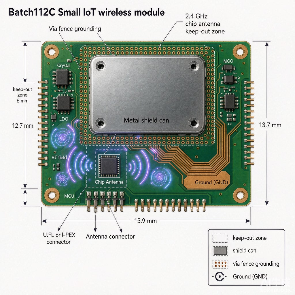
A board-level shield can (soldered stamped enclosure over the radio section) serves three purposes: contains the radio’s local oscillator and switching noise, blocks hostile noise from nearby power electronics, and stabilizes the radio’s environment against nearby metal changes. Placement rules:
- Shield the radio core, not the ante
a.
The can must stop before the antea keep-out. A common mistake is a single can over the whole module including the chip ante
a — radiated efficiency collapses.
- Wall height: 2–3 mm walls clear typical component heights; taller cans have slightly lower seam leakage but cost height budget.
- Via fencing: Stitch the can’s ground flange with vias every 2–3 mm (well under λ/20 at 2.4 GHz, which is 6.2 mm). A flange grounded only at corners leaks through the seams.
- Feedthrough filtering: Every signal leaving the can should pass a series element (bead or resistor) plus a shunt capacitor referenced to the fence. Power enters through a pi filter. Unfiltered can penetrations make the can decorative.
Grounding and Return Paths Inside the Module
At 2.4 GHz, return currents follow the ground plane directly under the trace. Design rules that matter:
- Keep the RF section on a solid, unsplit ground layer; a single 0.5 mm slot across a return path can turn a trace into a patch ante
a.
- Ground the crystal load capacitors, the PA decoupling, and the ante
a matching network to the same local ground island with short, wide co
ections.
- Keep switching regulators at least 10 mm from the ante
a matching network, or separate them with a shield wall. Buck converter harmonics land directly in the 2.4 GHz ISM band’s spurious limits.
- Co
ect any external chassis metal to board ground at one controlled point near the RF co
ector to avoid floating-metal re-radiation.
Regulatory Test Targets
For FCC/CE/ISED in the 2.4 GHz band, the failing measurements are usually: out-of-band spurious emissions from digital circuitry (24.25–24.45 GHz and below 2.4 GHz edges), conducted spurious on the ante
a port, and band-edge occupied bandwidth. Pre-compliance measures that catch 90% of issues:
- Near-field probe scans over the PCB to find leaking nets before the chamber visit.
- A 30 cm TEM-style fixture or bench spectrum measurement of conducted spurious on the ante
a feed.
- Testing with the enclosure on and the product in its worst real-world orientation — plastic housings are transparent at 2.4 GHz, but metal trim near the ante
a is not.
Common Failure Patterns and Fixes
- Shield can touching nearby component bodies: raises ground impedance unpredictably. Keep 1 mm clearance.
- Ante
a detuned after enclosure assembly:
add a matching-component pad set and re-match with the final housing; do not assume reference-design match survives a different enclosure. - Spurs from display flex cables ru
ing past the radio:
route the flex away, add ferrite clamp if unavoidable. - Intermittent range loss with wall adapters: common-mode noise on the DC input; fix with input common-mode filtering, not ante
a changes.
Design Sequence Summary
- Reserve ante
a keep-out per the vendor reference design — non-negotiable.
- Shield the radio core with a via-fenced can, filtered penetrations, and a solid ground layer.
- Separate switching noise sources spatially or with shield walls.
- Pre-scan with near-field probes; fix at the source.
- Re-match the ante
a with the final enclosure; validate band-edge performance.
Products that follow this sequence pass 2.4 GHz regulatory testing on the first or second chamber visit. Products that treat the ante
a layout loosely spend their schedule in test loops — the keep-out zone is the cheapest insurance in the whole design.