Why Thickness Tolerance Matters in SMT Stamping
Copper strip for SMT terminals, shield cans, and busbar tabs is typically ordered in thicknesses from 0.05 mm to 0.60 mm. What matters to a progressive die is not the nominal value but the tolerance band and how consistently the mill holds it. Thickness variation directly shifts the clearance between punch and die: a strip specified at 0.20 ±0.010 mm changes clearance by ±10% across the band. Too tight and the die burnishes and galls; too loose and the burr height grows and the fracture zone deepens. Both failure modes show up later as plating skips and contact resistance drift.
Tolerance Grades You Can Actually Buy
Standard mill tolerance
Conventional cold-rolled copper strip is supplied to ±5% of nominal thickness, which on 0.20 mm is ±0.010 mm. This is adequate for general brackets and EMI cans.
Precision and full-hard precision grades
For lead frames and spring contacts, specify precision-rolled strip at ±2.5% or better (±0.005 mm on 0.20 mm). High-end mills can offer ±1.5% on thin gauges with tension-leveling and online thickness gauges. The premium is typically 10–25%, trivial against the cost of a scrapped stamping run.
Camber and profile vs thickness
Thickness tolerance is often quoted at strip centerline. Profile variation—crown, wedge, and edge drop across the width—matters just as much for wide coils feeding multi-cavity dies. Ask the supplier for center versus edge measurements; a strip that is in-tolerance at center but 8 µm thi
er at the edges will produce different burr heights across the die.
How Gauge Is Measured and Reported
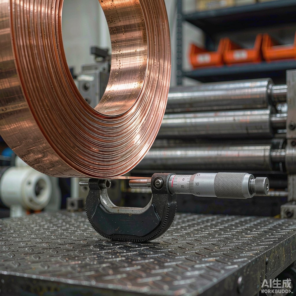
Mills measure with contact micrometers at defined points or with X-ray and laser gauges traversing the moving strip. Data should be delivered as a digital thickness profile per coil, not a single number on a certificate. For critical orders, request:
- Full-length min/max/mean thickness per coil
- Cross-profile readings at head, middle, and tail
- Statistical capability (Cp/Cpk) against your specified band, ideally Cpk ≥ 1.33
Receiving inspection should sample with a calibrated digital micrometer at 1 m intervals on the first and last 10 m of the coil, where thickness drift is most likely due to rolling setup transitions.
Thickness, Die Clearance, and Burr Height
For copper alloys, recommended punch-to-die clearance is 5–10% of strip thickness per side. When incoming strip runs 0.010 mm thick relative to nominal, the effective clearance percentage drops, raising punch force and burnish depth. The practical consequence is accelerated die wear and erratic burr height within a single coil. Plants that track burr height per coil often find the correlation with incoming thickness is stronger than with die age—evidence that gauge control belongs in incoming quality, not just die maintenance.
Plating and Assembly Consequences
Electroplating current density is set per unit area; thickness deviation changes the plated layer distribution at edges and corners. A strip at the thin end of the band gets proportionally heavier plating buildup on edges, risking sharp burrs on tin or silver coatings that abrade contacts. In ultrasonic and resistance welding of tabs, thickness variation alters weld energy settings—a batch that drifts 8% thick may need re-qualification of the weld schedule.
Writing a Practical Purchase Specification
- State nominal thickness with tolerance (e.g., 0.20 mm +0/−0.005 mm if the die prefers thin-side stock).
- Require cross-profile limits, not just centerline.
- Demand digital gauge data or a signed Cpk report per coil.
- Agree on sampling method for receiving inspection and arbitration (ASTM B224 or ISO 4316 practices).
Controlling strip thickness tolerance is one of the cheapest levers in SMT stamping quality: it stabilizes burr height, plating, and weld parameters across every coil you receive.