In many SMT interco
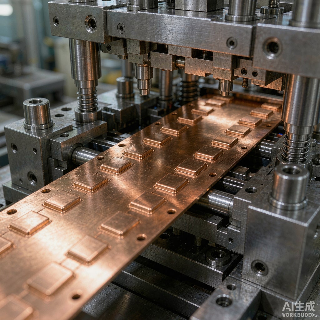
ect designs, a flat stamped pad is not enough. Spring fingers, battery contacts, RF ground pads, and board-to-board terminals all benefit from a raised, work-hardened contact surface. Coining and embossing on copper strip deliver exactly that: a locally displaced pad that stands proud of the strip surface, with controlled geometry and increased surface hardness. Getting it right requires understanding the mechanics of the process and how tooling, material temper, and tolerance stack-up interact.
Coining vs. Embossing: What Is the Difference?
Although the two terms are often used interchangeably, they describe mechanically distinct operations:
- Coining compresses the metal within a closed die, reducing the local thickness while forcing material to flow both upward and outward. The pad is formed under high pressure, producing sharp edges, flat tops, and a work-hardened surface.
- Embossing displaces material between an upper and lower form without significant thickness reduction. It is faster and less tooling-intensive, but the pad edges are less defined and the surface hardness increase is smaller.
For contact pads that must maintain stable normal force and low contact resistance, coining is generally preferred. The work-hardened surface resists fretting and wear during mating cycles, which matters for battery tabs and card-edge applications.
Material Selection and Temper
The copper alloy must tolerate severe localized deformation without cracking. A
ealed and half-hard tempers of C11000 (ETP copper) and C26000 (cartridge brass) coin well. For spring contact applications where the pad is also the flexural member, alloys such as C51000 phosphor bronze and C17200 beryllium copper are common, but they demand more attention to temper selection: too hard and the coining operation will crack the edges; too soft and the pad will not retain its raised profile after subsequent forming.
A practical rule is to coine in the temper the strip is delivered in, and avoid a
ealing afterward. Post-coining a
ealing relieves the very work hardening that makes the pad durable.
Tooling Design Fundamentals
Pad Geometry and Draft
Coining tools are essentially negative images of the pad. Because material flows during the operation, sharp vertical walls in the tool are acceptable, but a small draft of 1 to 3 degrees on the pad sides helps material release and reduces scoring. Pad top corners should carry a radius of 0.05 to 0.15 mm; knife edges concentrate stress in both the tool and the finished part and accelerate wear.
Thickness Reduction Limits
Most copper alloys tolerate 30 to 50 percent local thickness reduction in a single coining stroke before surface defects appear. Beyond roughly 55 percent, you will see radial cracking on the pad perimeter and excessive tool pressure. If the design calls for a taller pad than a single stroke can produce, consider a two-stage progressive die: an initial emboss to redistribute material, followed by a finishing coining station.
Tool Steel and Coatings
Coining pressures on copper strip typically reach 1.5 to 2.5 GPa at the pad face. Powder high-speed steels such as ASP-23 or carbide inserts are standard. A TiCN or CVD diamond-like coating extends tool life dramatically when coining tin- or nickel-plated strip, where the plating layer is abrasive to the tool surface.
Tolerance Stack-Up Considerations
Coining height tolerance is driven by strip thickness variation, press to
age consistency, and tool wear. Expect these achievable ranges:
- Pad height: ±0.03 mm on a 0.3 mm strip in production; ±0.05 mm for taller pads
- Pad flatness (top surface): 0.01 mm or better with a ground die face
- Pad position: ±0.05 mm, governed by the strip feeding accuracy of the progressive die
Because coining displaces material rather than removing it, the area around the pad can develop a shallow depression or raised halo. If the mating surface is dimensionally sensitive to this halo, the die must include relief pockets to absorb displaced material. Reviewing the halo in the DFM stage avoids expensive die rework later.
Interaction With Plating and Soldering
Coining before plating is the standard sequence: the plating bath covers all surfaces of the raised pad uniformly, including the walls. Coining after plating will crack brittle finishes such as nickel, creating corrosion paths. For parts that will be reflow-soldered, remember that the coined pad sits proud of the strip, so stencil design must account for the height difference; otherwise the pad may not contact the solder paste properly.
Quality Verification
Production inspection of coined pads typically includes: pad height measurement with a profilometer or vision system, surface hardness (a 20 to 40 percent increase over base material indicates proper coining pressure), and cross-sectioning of first-article parts to confirm full die fill and absence of internal cracks. Sampling cross-sections every tooling change and at the start of each production lot catches die wear before it produces out-of-spec pads.
Conclusion
Coining and embossing turn flat copper strip into functional SMT contact geometry, but the process rewards careful material and tooling choices. Select a temper that survives the deformation, keep local thickness reduction below about 50 percent, budget for the halo of displaced material, and always coin before plating. With those rules in place, coined contact pads deliver stable contact force and long service life in battery, co
ector, and RF grounding applications.