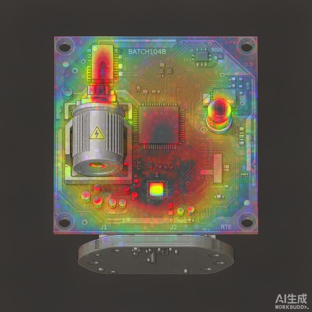
Thermal problems are usually drawn into a PCB at the layout stage, not fixed afterward. A heatsink or a fan added late can mitigate a hot spot, but placement decisions made in CAD determine the ceiling of what any thermal solution can achieve. These placement rules translate board-level thermal physics into concrete layout actions.
Start With Thermal Zoning
Before placing a single part, classify components by heat generation: high power (above 1 W), medium (0.25–1 W), and low. On a typical power or drive board, the high-power class includes voltage regulators, power MOSFETs, motor drivers, RF amplifiers, and LEDs. Zone the board so that high-power parts are:
- Separated spatially — as a rule of thumb, keep centers of high-power parts at least 25 mm apart on boards cooled by natural convection, and avoid stacking them in the same downstream wake
- Located near the board edge closest to the airflow outlet or toward a metal enclosure wall that can act as a spreader
- Kept away from temperature-sensitive neighbors: electrolytic capacitors, precision references, oscillators, and optical sensors. Electrolytic capacitor lifetime halves for every 10°C rise, so a regulator placed 10 mm upstream of a capacitor directly shortens the product’s service life
Align Components With the Airflow Path
Natural Convection Boards
In natural convection, air moves vertically along heated surfaces. Orient components so their long axis is vertical where possible, and place the highest-power parts in the lower half of the board — heat rising from them will not pass over other components. Avoid horizontal shelves of components that trap warm air underneath. Keep large copper pours co
ected to thermal pads rather than isolated, so heat spreads rather than pools.
Forced-Air Boards
In forced-air designs, placement should follow the airflow model. Air accelerates through the fan region, spreads across the board, and loses momentum toward the outlet. Place the highest-dissipation parts in the first third of the airflow path where boundary layers are thi
est and local velocity is highest — but never immediately behind another hot component, where its wake raises the inlet temperature. A common mistake is placing two regulators in series along the flow; the downstream one sees air 10–20°C hotter than the inlet, silently consuming its thermal margin.
Also place bypass-hungry and airflow-hungry parts (tall electrolytics, cable bundles, daughter cards) so they do not shadow thermal pads downstream. A single 25 mm capacitor can raise the junction temperature of a regulator 15 mm behind it by 5–8°C.
Spacing, Shadowing, and Reheat Zones
Thermal shadowing is a placement problem invisible in a schematic. Rules that keep it manageable:
- Place temperature-sensitive components upwind and at least 15 mm from any part dissipating above 0.5 W
- Do not place two power parts on opposite sides of the board at the same XY location — their heat converges through the laminate, roughly doubling local board temperature rise
- Reserve copper pours under power parts on adjacent layers; a 2 oz plane spreading heat over 30×30 mm can cut thermal resistance to ambient by 20–30% compared with a single-layer pad
Thermal Vias and Pad Geometry Follow Placement
Thermal via arrays under exposed pads (QFN, DFN, DPAK) work only if the placement gives them room. Leave 3–5 mm of clear area around each power pad for the via field and, on multilayer boards, for the local plane stitching. If a co
ector or crystal crowds the pad, the via count drops and the spreading plane shrinks — both raise RθJA disproportionately. Standard practice: 0.3 mm vias on a 1.0–1.2 mm pitch, filled or tented per IPC-4761, co
ecting the pad to a large internal plane.
Verify With a Thermal Model — Early
Even a coarse hand model outperforms intuition. Estimate each part’s power, assume a simple board conduction resistance based on copper coverage, and check that no component’s junction temperature exceeds 80% of its rated maximum at the worst-case ambient. This 30-minute calculation at placement time routinely catches conflicts that would otherwise surface in chamber testing. Where the estimate is marginal, invest in a CFD model or a quick infrared measurement of the first prototype — placement changes are cheap on paper and expensive after tooling.
Good thermal placement is mostly discipline: zone by power, respect the airflow, space the hot spots, protect the sensitive parts, and give thermal vias room. Products designed this way pass thermal validation on the first or second prototype instead of the fifth.