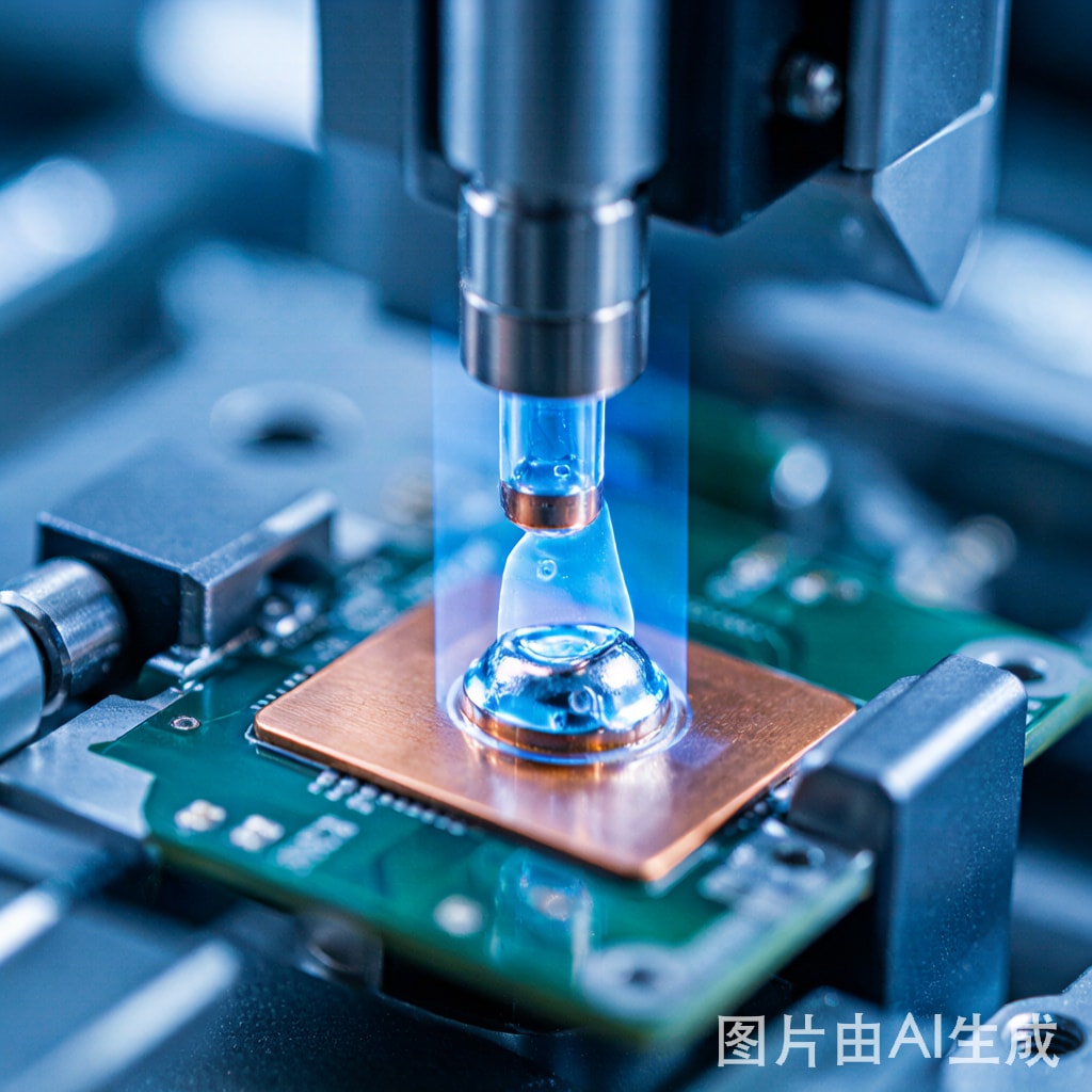
As power densities in modern SMT assemblies continue to rise, the quality of solder joints beneath large copper thermal pads has become a critical reliability concern. Void formation during reflow soldering can reduce thermal conductivity by up to 40%, creating localized hotspots that accelerate device degradation and early field failures.
Vacuum reflow soldering has emerged as the most effective process solution for achieving void-free solder joints on high-power SMT assemblies with copper thermal pads. This article examines the technology, process parameters, and verification methods that define best-in-class void control.
Understanding Void Formation in Thermal Pad Soldering
Solder voids form when entrapped gases—primarily flux volatiles and air—ca
ot escape the molten solder before solidification. The problem is particularly severe for large-area thermal pads, where the escape path for gases is long relative to the solder joint thickness.
Three primary mechanisms contribute to void formation:
- Flux outgassing: Flux activators decompose during the reflow soak and peak zones, releasing volatile compounds that must vent through the liquid solder.
- Entrapped air: Air pockets trapped between the PCB pad and component during placement become sealed when the solder paste coalesces.
- Moisture vaporization: Absorbed moisture in PCB laminate and component packages expands rapidly at soldering temperatures, creating steam bubbles.
IPC-7093 classifies voids into macro-voids (>25% of pad area) and micro-voids (5–25%), with Class 3 high-reliability applications requiring total void area below 15% for thermal pads.
The Vacuum Reflow Process
Vacuum reflow soldering introduces a controlled low-pressure phase during the liquidus period of the reflow profile, after full solder melting but before cool-down begins.
Process Sequence
- Atmospheric reflow ramp: Standard convection reflow through preheat, soak, and ramp-to-peak zones under nitrogen atmosphere (oxygen < 500 ppm).
- Wetting dwell: A 15–30 second hold above liquidus (typically 230–240°C for SAC305) to ensure complete solder coalescence and wetting.
- Vacuum pulse: Chamber pressure reduced to 10–50 mbar (1–5 kPa) for 10–30 seconds. The pressure differential causes trapped gas bubbles to expand dramatically (Boyle’s law), overcoming surface tension and rising to the surface.
- Atmospheric release: Chamber vented back to atmospheric pressure, collapsing any remaining micro-voids.
- Controlled cooling: Cooling ramp of 2–4°C/s to solidify the now void-free solder joint.
Critical Process Parameters
| Parameter | Recommended Range | Impact |
|---|---|---|
| Vacuum level | 10–50 mbar | Lower pressure = greater void collapse force |
| Vacuum duration | 10–30 seconds | Longer = more complete outgassing; too long = excessive solder oxidation |
| Vacuum onset timing | 5–10s after peak | Too early = incomplete wetting; too late = partial solidification |
| Oxygen residual | <100 ppm | Lower O₂ prevents re-oxidation of exposed solder surface |
Efficacy for Copper Thermal Pads
Copper thermal pads present unique challenges due to their high thermal mass and large surface area (typically 5–50 mm² for power packages like QFN, TOLL, and DPAK). The high thermal conductivity of copper (398 W/m·K) means the pad acts as a heat sink, potentially creating temperature gradients that trap gases at the pad center.
Independent studies have demonstrated that vacuum reflow reduces average void percentage from 15–35% (atmospheric reflow) to below 2% for copper thermal pads larger than 20 mm². At 50 mbar vacuum, the void collapse efficiency exceeds 95% for SAC305 solder.
X-Ray Verification and IPC-7093 Compliance
Post-reflow X-ray inspection is essential for void verification. 2D X-ray provides area-percentage void measurement; 3D computed tomography (CT) X-ray reveals void distribution through the solder joint thickness—critical because stacked voids at the pad-solder interface have disproportionately large thermal impact.
IPC-7093D specifies acceptance criteria: Class 1 (general electronics) allows up to 30% void area; Class 2 (dedicated service) up to 20%; and Class 3 (high reliability) up to 15% for thermal pads. Vacuum reflow consistently achieves Class 3 compliance with margin.
Conclusion
For manufacturers of high-power SMT assemblies using copper thermal pads, vacuum reflow soldering represents a mature, production-ready solution for void elimination. When combined with proper stencil design, optimized reflow profile, and X-ray verification, vacuum reflow delivers the thermal and mechanical reliability demanded by automotive, industrial, and aerospace power electronics applications.



