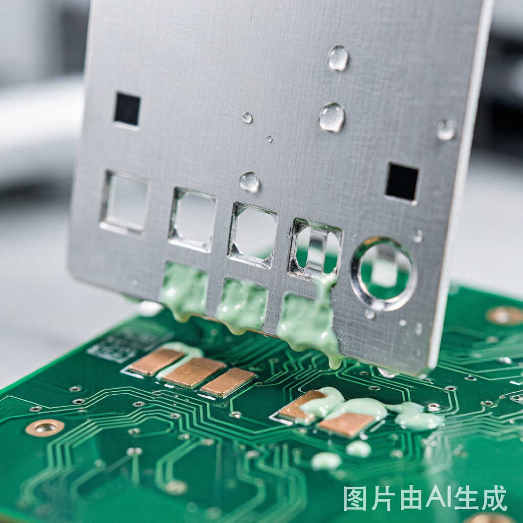
As SMT component pitches shrink below 0.4 mm, the area ratio of stencil apertures decreases to levels where solder paste release becomes the dominant factor in print quality. For copper pads on high-density PCBs, incomplete paste transfer leads to insufficient solder volume, open joints, and reduced first-pass yield.
SMT stencil nano-coating technology has emerged as a game-changing solution, applying microscopic functional coatings that dramatically improve paste release without affecting aperture dimensions. This article examines the technology, performance benefits, and implementation considerations.
The Area Ratio Challenge
Solder paste release from stencil apertures follows a straightforward physical principle: the paste must adhere more strongly to the PCB pad than to the stencil aperture walls. The area ratio—defined as the aperture opening area divided by the aperture wall area—is the primary predictor of release performance:
Area Ratio = (L × W) / (2 × (L + W) × T)
Where L and W are aperture dimensions and T is stencil thickness. Industry guidelines recommend an area ratio above 0.66 for reliable paste transfer. For a 0.3 mm × 0.3 mm aperture in a 0.1 mm thick stencil, the area ratio is 0.75—marginally acceptable. But for a 0.2 mm × 0.2 mm aperture at the same thickness, the area ratio drops to 0.50, well below the reliable transfer threshold.
Nano-Coating Technology Fundamentals
Nano-coatings for SMT stencils are typically fluoropolymer-based treatments applied at thicknesses of 50–200 nanometers—one to two orders of magnitude thi
er than traditional stencil coatings. Two primary technologies dominate the market:
1. Plasma-Enhanced Chemical Vapor Deposition (PECVD)
PECVD deposits a conformal fluorocarbon film in a low-temperature plasma chamber. The process creates covalent bonds between the coating and the stainless steel stencil surface, providing exceptional durability (100,000+ print cycles before re-coating).
2. Liquid-Phase Dip Coating
A self-assembled monolayer (SAM) of fluorinated silane molecules is applied via dip coating and thermal curing. The molecules orient with their fluorinated tails pointing outward, creating an ultra-low-energy surface. Dip coating is more economical but has a shorter service life (20,000–50,000 cycles).
Performance Benefits
| Metric | Uncoated Stencil | Nano-Coated Stencil | Improvement |
|---|---|---|---|
| Contact angle (water) | 70–85° | 110–130° | Superior repellency |
| Surface energy | 35–45 mN/m | 12–18 mN/m | 2–3× reduction |
| Area ratio threshold | 0.66 minimum | 0.45 minimum | Extends usable range |
| Paste transfer efficiency | 80–90% | 95–99% | Significant gain |
| Under-stencil cleaning frequency | Every 5–10 prints | Every 50–100 prints | 5–10× longer |
Benefits for Copper Pad Applications
Copper pads present specific challenges that nano-coatings address effectively:
Oxide layer mitigation: Bare copper pads develop a native oxide layer (Cu₂O) within hours of PCB fabrication, reducing surface energy and solder paste adhesion. Nano-coated stencils compensate for this reduced pad receptivity by maximizing paste release from the aperture side.
OSP-finished pads: Organic Solderability Preservative (OSP) finishes on copper pads provide a thin, uniform organic barrier. However, OSP coatings vary in thickness and quality across PCB suppliers. Nano-coated stencils provide consistent paste transfer independent of minor pad surface variations.
Fine-pitch QFN and LGA pads: For 0.4 mm pitch QFN packages with 0.2 mm wide copper pads, nano-coating technology consistently achieves transfer efficiency above 95%, compared to 75–85% for uncoated stencils.
Implementation Considerations
When adopting nano-coated stencils, manufacturers should consider:
- Stencil cleaning: Use solvent-based cleaners compatible with fluoropolymer coatings. Alcohol-based wipes can degrade some dip-coated surfaces over time.
- Squeegee compatibility: Metal squeegee blades are recommended; polyurethane blades may experience increased wear against the low-friction surface.
- Storage: Store nano-coated stencils in a clean, dry environment. The hydrophobic surface naturally repels moisture and contaminants.
- Cost-benefit analysis: While nano-coated stencils cost 30–60% more than uncoated stencils, the reduction in defects, cleaning frequency, and stencil replacement cycles typically yields ROI within 3–6 months for high-volume production.
Conclusion
Nano-coating technology represents a proven, cost-effective upgrade for SMT stencil printing of fine-pitch copper pad assemblies. By reducing the effective area ratio threshold, improving paste transfer consistency, and extending cleaning intervals, nano-coated stencils deliver measurable improvements in first-pass yield and overall equipment effectiveness in modern SMT production lines.



