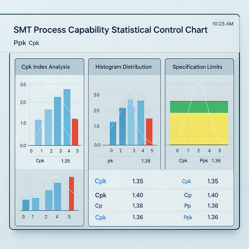
## Why Process Capability Matters in SMT Manufacturing
Process Capability Index (Cpk) quantifies how well a manufacturing process produces output within specification limits. In SMT electronics manufacturing, two parameters dominate quality outcomes: solder paste deposit volume (which determines joint formation, void content, and intermetallic thickness) and copper component thickness (which controls current capacity, thermal resistance, and mechanical fit in co
ector sockets). When these parameters drift beyond their specification windows, the downstream consequences are solder defects, electrical failures, and dimensional non-conformance that escalate rework cost and reduce production yield.
Cpk analysis transforms raw measurement data into a single actionable number. A Cpk of 1.33—the minimum threshold for capable processes per AIAG SPC guidelines—means the process average is centered within specification limits with enough margin that only 0.006% of production (63 parts per million) falls outside specification. A Cpk below 1.00 indicates the process produces more than 0.27% defective output (2,700 ppm)—an unacceptable defect rate for most SMT applications. Understanding how to calculate, interpret, and improve Cpk for solder volume and copper thickness enables systematic quality improvement rather than reactive defect firefighting.
## Solder Paste Volume Cpk Analysis
### Specification Limits and Measurement Method
Solder paste volume specification is derived from stencil aperture design and IPC-7527B guidelines. The target volume (V_target) is calculated from the aperture area × stencil thickness, with upper and lower specification limits (USL/LSL) typically set at ±25% to ±40% of target, depending on component type:
| Component Type | Target Volume Tolerance | USL | LSL | Rationale |
|—————|————————|—–|—–|———–|
| Chip component (0402–0603) | ±25% | V×1.25 | V×0.75 | Tombstone sensitivity at low volume |
| QFN/BGA center pad | ±40% | V×1.40 | V×0.60 | Void tolerance allows wider window |
| Fine-pitch QFP (≤0.5mm) | ±20% | V×1.20 | V×0.80 | Bridge risk at high volume |
| Large BGA (≥1.0mm pitch) | ±30% | V×1.30 | V×0.70 | Sufficient paste for joint formation |
Solder paste volume measurement uses 3D solder paste inspection (SPI) systems that scan each deposit with structured light or laser triangulation, producing height maps with 1–5 μm vertical resolution. Volume calculation integrates the height map over the aperture area: V = ∫∫h(x,y)dx·dy, where h(x,y) is the measured height at each pixel coordinate. Modern SPI systems measure 100% of deposits on every board, generating massive datasets that feed directly into SPC analysis.
### Cpk Calculation and Interpretation
Cpk for solder paste volume uses the standard formula:
Cpk = min[(USL – μ) / (3σ), (μ – LSL) / (3σ)]
Where μ is the process mean (average volume across all deposits) and σ is the process standard deviation (volume variation across deposits).
A practical example for 0603 chip component paste deposits:
– Target: 4500 μm³ (0.25 mm × 0.15 mm aperture × 0.12 mm stencil)
– USL: 5625 μm³ (+25%)
– LSL: 3375 μm³ (-25%)
– Measured μ: 4700 μm³ (slightly above target)
– Measured σ: 320 μm³
Cpk_upper = (5625 – 4700) / (3 × 320) = 925 / 960 = 0.96
Cpk_lower = (4700 – 3375) / (3 × 320) = 1325 / 960 = 1.38
Cpk = min(0.96, 1.38) = 0.96 → Process is NOT capable (below 1.33)
The calculation reveals the root cause: the process mean is shifted above target, consuming upper specification margin. The lower specification has ample margin (1.38), but the upper margin is insufficient (0.96). This asymmetric result—common in solder paste SPC—directs corrective action toward reducing the mean shift rather than reducing variation.
### Common Cpk Failure Modes for Solder Volume
| Failure Mode | Cpk Pattern | Root Cause | Corrective Action |
|————-|————|———–|——————-|
| Mean shift up | Cpk_U << Cpk_L | Stencil over-printing, aperture wear | Reduce stencil thickness or aperture size |
| Mean shift down | Cpk_L << Cpk_U | Under-printing, stencil clogging | Clean stencil, verify paste rheology |
| High σ, centered mean | Cpk_U ≈ Cpk_L < 1.33 | Excessive variation | Improve paste consistency, stabilize environment |
| Asymmetric limits | Different margins | Non-uniform aperture design | Optimize aperture area ratio per IPC-7527B |
| Batch-to-batch drift | Cpk varies by time | Paste viscosity aging, stencil wear | Schedule paste replacement, track stencil life |
## Copper Strip Thickness Cpk Analysis
### Specification Framework
Copper strip thickness for SMT lead frames, EMI shielding cans, and bus bar products follows tolerance specifications defined by alloy standard (ASTM B152 for flat copper products) and customer drawing requirements:
| Application | Nominal Thickness | Standard Tolerance | Typical USL/LSL | Critical Parameter |
|————-|——————|——————-|—————–|——————-|
| SMT lead frame | 0.15 mm | ±0.010 mm | 0.160/0.140 mm | Die attach bond line |
| EMI shielding can | 0.20 mm | ±0.015 mm | 0.215/0.185 mm | Shielding effectiveness |
| Bus bar power | 0.50 mm | ±0.025 mm | 0.525/0.475 mm | Current capacity margin |
| Co
ector contact | 0.10 mm | ±0.005 mm | 0.105/0.095 mm | Contact force consistency |
Thickness measurement uses micrometer gauges (resolution 0.001 mm) or laser thickness gauges (resolution 0.0005 mm) in continuous strip production, sampling at 1-meter intervals. For discrete stamped parts, optical measurement systems provide thickness data at multiple points per piece.
### Cpk Calculation Example
For 0.15 mm C19400 lead frame strip:
– Nominal: 0.150 mm
– USL: 0.160 mm (+0.010 mm)
– LSL: 0.140 mm (-0.010 mm)
– Measured μ: 0.151 mm (slightly above nominal)
– Measured σ: 0.003 mm (good consistency from rolling mill)
Cpk_upper = (0.160 – 0.151) / (3 × 0.003) = 0.009 / 0.009 = 1.00
Cpk_lower = (0.151 – 0.140) / (3 × 0.003) = 0.011 / 0.009 = 1.22
Cpk = min(1.00, 1.22) = 1.00 → Marginal capability
The process meets the 1.00 minimum but falls short of the 1.33 capability target. The mean shift of 0.001 mm above nominal—barely detectable in absolute terms—reduces Cpk from a potential 1.11 (if centered) to 1.00. This illustrates a critical SPC principle: in tight-tolerance copper thickness applications, even microscopic mean shifts consume capability margin.
## Sampling Strategy and Measurement Frequency
### Solder Paste Volume Sampling
For 100% SPI inspection (recommended for Class 3 per IPC-A-610), every paste deposit on every board contributes to the Cpk calculation. This generates thousands of data points per board—enough for stable σ estimation within a single production run. However, three sampling pitfalls require attention:
1. Pad size grouping: Cpk must be calculated separately for each aperture size category. Mixing 0603 and QFN center pad volumes in one dataset produces misleading σ values that blend two distinct populations
2. Board position effect: Paste volume varies across the stencil area (edge deposits typically 5–10% lower than center deposits due to squeegee pressure distribution). Calculate position-stratified Cpk to detect this systematic variation
3. Temporal stability: Cpk calculated from a single production run may not represent long-term capability. Track Cpk across multiple shifts, paste batches, and stencil life cycles to capture long-term variation sources
### Copper Thickness Sampling
Copper strip thickness sampling follows a different strategy because the measurement is continuous (in-line production) rather than discrete (board-by-board):
– In-line laser gauge: Continuous measurement at 1 m intervals, providing 100+ readings per coil. This enables real-time Cpk calculation per coil with automatic rolling mill adjustment
– Piece-by-piece measurement: For stamped SMT parts, 5-piece samples per 500-piece lot (per ASTM E122) provide sufficient statistical power for Cpk estimation when σ is stable
– Multi-point measurement: Each piece measured at 3 positions (edge, center, opposite edge) to capture cross-strip thickness variation, which can differ from along-strip variation
## Corrective Action Framework
When Cpk falls below the 1.33 threshold, the corrective action depends on which component of the Cpk formula is deficient:
| Cpk Condition | Diagnosis | Primary Action | Secondary Action |
|—————|———–|—————|—————–|
| Mean shift only (Cp ≥ 1.67, Cpk < 1.33) | Process centered incorrectly | Adjust process target (stencil, mill settings) | Verify measurement calibration |
| High variation (Cp < 1.33) | σ too large for specification width | Identify and reduce dominant variation source | Widen specification if justified |
| Both mean shift + high variation | Process out of control | First: stabilize process (reduce σ), then: recenter | Full SPC investigation required |
| Cpk degrading over time | Progressive wear or drift | Replace worn tooling (stencil, mill rolls) | Schedule preventive maintenance |
The key principle: never widen specification limits to improve Cpk. Specification limits represent real engineering requirements—solder volume limits are derived from defect physics (tombstone, bridge, void), and copper thickness limits are derived from functional requirements (current capacity, mechanical fit). Artificially widening limits improves the Cpk number while compromising the product quality that Cpk was designed to protect.
## Conclusion
Cpk analysis provides the statistical framework for quantifying SMT process quality in solder paste volume and copper component thickness. The methodology is straightforward—measure μ and σ, compare against engineering-derived specification limits, and calculate the minimum distance from process average to specification boundary in units of process variation. The challenge lies not in the math but in the discipline: maintaining consistent measurement, stratifying data by relevant categories, tracking capability over time, and taking corrective action based on Cpk diagnosis rather than arbitrary specification widening. A Cpk ≥ 1.33 for both solder volume and copper thickness is the minimum quality foundation for reliable SMT manufacturing—anything less demands immediate investigation and process improvement.



