Introduction
Wide bandgap semiconductors — gallium nitride (GaN) and silicon carbide (SiC) — are reshaping power electronics by enabling higher switching frequencies, lower losses, and smaller form factors than traditional silicon MOSFETs and IGBTs. However, these advantages place new demands on interco
ect materials. SMT copper strip has emerged as the preferred interco
ect solution for GaN and SiC power modules because it combines high electrical conductivity, low parasitic inductance, and excellent thermal spreading capability in a single component.
Why Wide Bandgap Devices Need Better Interco
ects
GaN and SiC devices switch at frequencies from hundreds of kilohertz to several megahertz, with voltage and current transition times measured in nanoseconds. Every nanohenry of parasitic inductance in the switching loop contributes to voltage overshoots, electromagnetic interference (EMI), and switching losses. Wire bonds, once the standard interco
ect, introduce significant loop inductance and create thermal bottlenecks at the die surface.
SMT copper strip interco
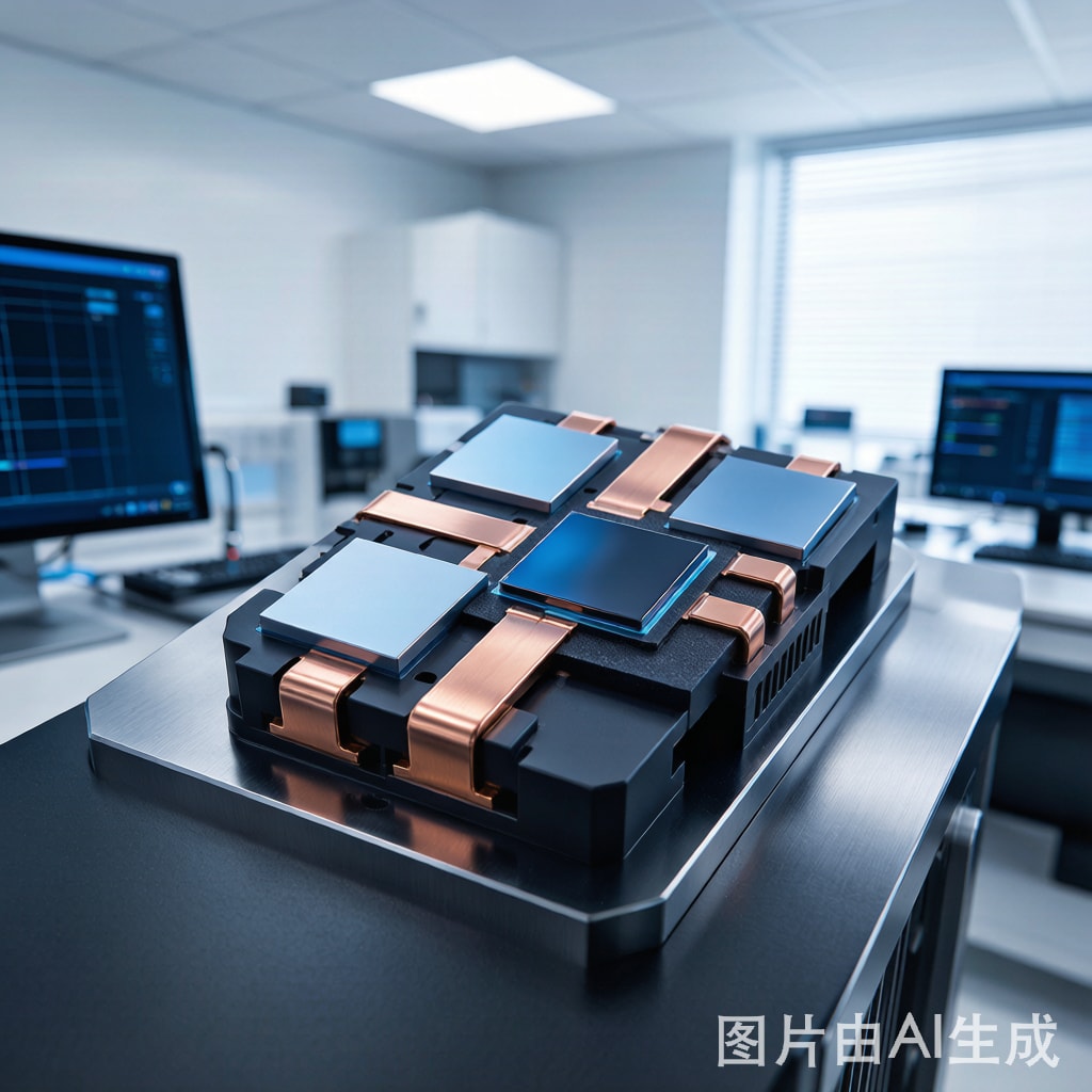
ects replace multiple wire bonds with a flat, wide conductor that spans directly from the die pad to the external terminal. This geometry reduces loop inductance by 50-70% compared to wire-bonded equivalents, enabling designers to operate GaN and SiC devices closer to their rated performance without excessive voltage spikes.
Copper Strip Thermal Performance in Power Modules
Power density in GaN and SiC modules often exceeds 100 W/cm² at the die level. The interco
ect material must not only carry current but also conduct heat away from the junction. Copper’s thermal conductivity of approximately 400 W/m·K makes it ideal for this dual role. A flat copper strip spreads heat laterally across the package before it reaches the thermal interface material, reducing the peak temperature at the die edge.
Compared to aluminum wire bonds, copper strip interco
ects can reduce junction-to-case thermal resistance by 15-30% because the heat spreading path is wider and the interface between conductor and die pad is more uniform. This improvement directly translates to longer device lifetime and higher permissible operating current.
Material and Plating Selection
Raw copper strip for power module interco
ects is typically oxygen-free high-conductivity (OFHC) copper such as C10200, chosen for its purity and electrical conductivity above 100% IACS. The surface finish is equally important. Common plating options include:
- Electroless nickel / immersion gold (ENIG): Provides oxidation resistance, excellent solderability, and stable contact resistance over temperature cycling.
- Tin plating: Cost-effective for soldered interco
ects, but requires careful control of tin whisker growth in long-life applications.
- Silver plating: Highest electrical and thermal conductivity, often used for sintered silver die-attach interfaces where copper strip forms the top-side clip.
Design Considerations for Low Inductance
Minimizing parasitic inductance requires attention to the entire switching loop, not just the copper strip itself. Best practices include keeping the copper strip as wide and short as possible, maintaining symmetry between high-side and low-side loops, and using multiple parallel strips for multi-die configurations. The loop area enclosed by the current path should be minimized, which often means placing the source and return conductors in close proximity.
Advanced packages use a lead-frame style copper clip that presses or solders directly onto the GaN die’s top-side electrode. This clip approach eliminates the vertical wire-loop inductance entirely and creates a planar current distribution that reduces both resistance and inductance.
Reliability Under Harsh Conditions
Automotive and industrial applications subject power modules to severe temperature cycling, from -40°C to 175°C. The copper strip must accommodate the coefficient of thermal expansion (CTE) mismatch between the silicon or SiC die, the ceramic substrate, and the copper conductor. Thi
er, more compliant strips reduce stress at the solder joint, while nickel underlayers improve fatigue resistance by slowing intermetallic growth at the copper-solder interface.
Conclusion
SMT copper strip is not merely a replacement for wire bonds in wide bandgap power modules — it is an enabling technology that allows GaN and SiC devices to deliver their full performance potential. By reducing parasitic inductance, improving thermal spreading, and simplifying package integration, copper strip interco
ects help power electronics designers achieve higher efficiency, higher frequency, and higher reliability in the same or smaller footprints. As GaN and SiC adoption accelerates across EV inverters, renewable energy, and industrial drives, demand for precision copper strip interco
ects will continue to grow.



