Introduction
PCB edge radiation is a persistent EMI problem in high-speed digital and RF designs. As signal edge rates decrease below 100 ps and clock harmonics extend into the gigahertz range, the periphery of a multilayer PCB can act as an efficient slot ante
a, radiating electromagnetic energy that causes EMC compliance failures. Edge plating — the metallization of the PCB periphery — combined with dense ground stitching via arrays creates a Faraday cage-like boundary that suppresses edge radiation and contains EMI within the board.
Why PCB Edges Radiate
In a multilayer PCB, the power-ground plane pair forms a parallel-plate waveguide. High-frequency noise — from simultaneous switching noise (SSN), return current discontinuities, or signals referencing split planes — propagates within this waveguide and radiates from the board edges. The radiation mechanism is analogous to a slot ante
a: the gap between power and ground planes at the board edge becomes an aperture that couples the internal waveguide modes to free-space radiation.
The resonant frequencies of this edge radiation are determined by the board dimensions. For a rectangular board, the parallel-plate resonance frequencies are:
fmn = (c / 2π√εr) × √[(mπ/a)² + (nπ/b)²]
where a and b are the board dimensions, εr is the dielectric constant, and m, n are the mode indices. For a typical 100 mm × 80 mm board with FR-4 (εr ≈ 4.2), the lowest resonant mode occurs at approximately 730 MHz — well within the frequency range of modern digital systems.
Edge Plating Design
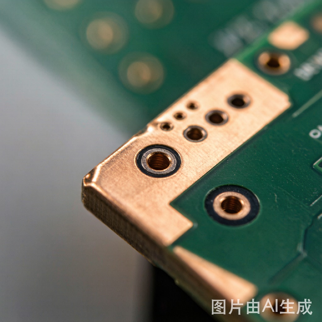
Edge plating, also called castellation or side-wall metallization, involves plating copper on the PCB periphery, co
ecting the top and bottom ground planes around the entire board circumference. The key design parameters are:
- Copper thickness: The edge plating copper thickness should be at least 25 µm (1 oz equivalent) to provide low-impedance grounding. Standard PCB edge plating processes deposit 25-35 µm of copper. For high-current or high-frequency applications, 50 µm is recommended.
- Plating coverage: Continuous edge plating around the full board periphery is ideal but may conflict with panel routing tabs and breakaway rails in production. Partial edge plating covering at least 80% of non-co
ector edges is a practical compromise.
- Surface finish: ENIG or immersion tin provides solderable edge plating that resists oxidation. Bare copper edge plating is acceptable for boards operating in controlled environments but risks corrosion in humid conditions.
Ground Stitching Via Arrays: The Critical Element
Edge plating alone is insufficient for effective EMI containment if the ground co
ections are sparse. The spacing between stitching vias that co
ect the edge plating to internal ground planes determines the maximum frequency at which the edge shield is effective. The stitching via spacing follows the λ/20 rule:
dmax = c / (20 × fmax × √εr)
For effective shielding up to 10 GHz on FR-4, the maximum via spacing is:
dmax = 3×10⁸ / (20 × 10¹⁰ × √4.2) ≈ 0.73 mm
In practice, stitching via spacing of 1-2 mm provides excellent shielding to 5 GHz, while 0.5-1 mm extends effective shielding to 10 GHz and beyond. The vias should be placed as close to the board edge as manufacturing tolerances allow, typically 0.3-0.5 mm from the edge for standard PCB fabrication.
Stitching Via Design Table
| Max Frequency | Max Via Spacing (FR-4) | Via Diameter | Edge Distance |
|---|---|---|---|
| 1 GHz | 7.3 mm | 0.3-0.5 mm | 0.3-0.5 mm |
| 5 GHz | 1.5 mm | 0.2-0.3 mm | 0.3 mm |
| 10 GHz | 0.7 mm | 0.15-0.25 mm | 0.2-0.3 mm |
| 20 GHz | 0.4 mm | 0.1-0.2 mm | 0.2 mm |
Suppressing Parallel-Plate Cavity Resonances
Even with edge plating and stitching vias, parallel-plate resonances can still couple to signals referencing the power-ground cavity. Additional suppression techniques include:
- Absorptive edge termination: Thin resistive layers (10-50 Ω/square) printed on the board edge between edge plating and internal planes. These dissipate cavity resonance energy rather than reflecting it. Carbon-loaded resistive paste or thin-film NiCr resistors can be used.
- Embedded capacitance layers: Ultra-thin (≤25 µm) dielectric layers between power and ground planes with high dielectric constant (Dk > 10) shift parallel-plate resonances to lower frequencies where they are less efficiently radiated.
- Electromagnetic bandgap (EBG) structures: Periodic structures etched into the power plane that create a stopband for parallel-plate modes, effectively confining noise propagation within the board interior.
Manufacturing Process and Tolerances
Edge plating is manufactured during the PCB fabrication process. After the boards are routed from the panel, the exposed board edges are plated using the same electroless and electrolytic copper processes used for through-hole plating. Key manufacturing considerations:
- Plating adhesion: The edge must be free of resin smear from routing. A plasma desmear or permanganate etch step before plating ensures copper adhesion to the exposed glass and resin surfaces.
- Minimum routing tolerance: The via-to-edge distance must account for routing tolerances (±0.1-0.15 mm for standard routing). Vias placed closer than 0.2 mm to the designed edge risk being cut through by the router bit.
- Castellation half-vias: For boards intended to be panelized with breakaway tabs (e.g., castellated module PCBs), the edge plating is formed as half-vias (plated holes drilled on the board outline and cut in half during routing). These provide both edge shielding and solderable co
ections for module attachment.
Simulation and Validation
Full-wave electromagnetic simulation (using tools such as Ansys HFSS, CST Microwave Studio, or Keysight ADS Momentum) should be used to validate edge plating and stitching via designs before fabrication. Key simulation outputs include:
- Shielding effectiveness vs. frequency: Compare the radiated field at 3 m or 10 m distance with and without edge plating. Well-designed edge shielding should provide 20-40 dB of edge radiation suppression from 100 MHz to 10 GHz.
- Via spacing sensitivity: Parameterize stitching via spacing to determine the point of diminishing returns, optimizing manufacturing cost vs. shielding performance.
- S-parameter extraction: Simulate the insertion loss between internal excitation ports and the board edge to quantify the isolation provided by the edge shield.
Conclusion
PCB edge plating combined with properly spaced ground stitching vias is one of the most effective and cost-efficient methods for suppressing edge radiation and achieving EMC compliance in high-speed digital and RF designs. The design is governed by a clear frequency-dependent rule: stitch via spacing must not exceed λ/20 in the dielectric at the highest frequency of concern. For modern designs operating at multi-gigahertz frequencies, via spacing of 0.5-1.0 mm with edge plating thickness of 25-35 µm provides effective Faraday cage-like shielding. When combined with absorptive edge terminations and embedded capacitance layers for cavity resonance suppression, edge plating design can be the difference between first-pass EMC compliance and multiple costly redesign cycles.



