Introduction
As power density increases in modern electronics, predicting copper trace temperature rise has become a critical part of PCB design. Traditional rules of thumb based on IPC-2152 provide a starting point, but they ca
ot account for the complex heat transfer paths in multilayer boards, adjacent components, and localized copper pours. Thermal simulation bridges this gap, enabling engineers to identify hotspots before prototyping.
Why Trace Temperature Rise Matters
Every copper trace has electrical resistance, and when current flows, resistive losses generate heat. The temperature rise above ambient depends on current magnitude, trace cross-section, copper resistivity, and the thermal environment. A trace that operates too hot can degrade solder joint reliability, accelerate insulation aging, and cause nearby components to exceed their maximum junction temperatures.
In high-current SMT applications, such as motor drivers, LED drivers, and power converters, localized trace heating can exceed 50°C above ambient. Without simulation, these hotspots are often discovered only during thermal testing, leading to expensive redesigns and schedule delays.
Key Parameters in Thermal Simulation
Accurate thermal simulation requires correct material properties and boundary conditions. The most important parameters include:
- Copper thermal conductivity: Approximately 398 W/m·K for pure copper, though plated or alloyed traces may differ slightly.
- FR-4 thermal conductivity: Typically 0.3 W/m·K in-plane and 0.25 W/m·K through-plane, making the substrate a poor heat spreader.
- Copper resistivity temperature coefficient: 0.00393 per °C — resistance increases as temperature rises, creating a feedback loop.
- Convection coefficient: Natural convection to still air is approximately 5-25 W/m²·K, while forced air can reach 50-150 W/m²·K.
- Boundary conditions: Fixed ambient temperature, component heat dissipation, and adjacent copper areas all influence the result.
From Analytical Models to Finite Element Analysis
Simple analytical models assume a uniform trace in free air with one-dimensional heat transfer. IPC-2152 provides empirical curves derived from such models, but they tend to be conservative for complex boards. For a first-order estimate, a 1 oz (35 µm) trace carrying 1 A per 0.5 mm of width typically produces a 10-20°C rise, depending on copper thickness and environment.
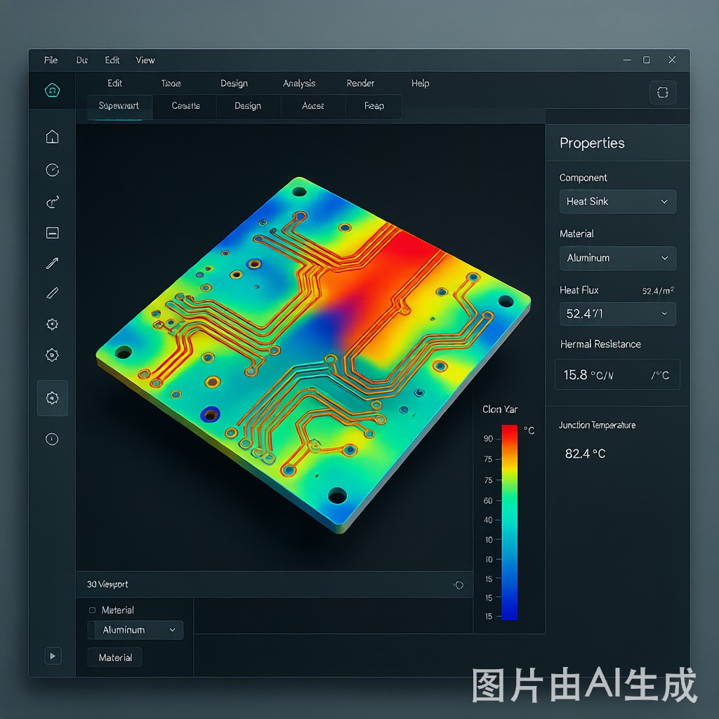
Finite element analysis (FEA) tools such as Ansys Icepak, Cadence Celsius, and open-source solvers can model the entire PCB geometry including trace patterns, component bodies, vias, and airflow. These simulations solve the coupled electrical-thermal problem, accounting for joule heating, conduction through the board, and convection to the surrounding air. The result is a detailed temperature map showing hotspots at trace necks, via arrays, and component pads.
Example Simulation Results for a 2 oz Trace
| Trace Width | Current | Ambient | Predicted ΔT |
|---|---|---|---|
| 1 mm | 5 A | 25°C | ~38°C |
| 2 mm | 5 A | 25°C | ~18°C |
| 3 mm | 5 A | 25°C | ~12°C |
| 1 mm | 10 A | 25°C | ~110°C |
Practical Design Guidelines
Simulation results should guide design decisions, not replace engineering judgment. Keep high-current traces short and wide, and avoid narrow necks that create localized heating. Use thermal vias beneath hotspots to conduct heat to internal or bottom copper layers, and place copper pours on multiple layers to improve heat spreading.
When simulations predict temperature rises above 40°C, consider adding external heatsinking, increasing copper weight, or using aluminum or copper-core substrates. For cost-sensitive designs, always validate simulation results with thermocouple measurements on physical prototypes, since material properties and boundary conditions can vary significantly between suppliers.
Conclusion
PCB copper trace thermal simulation is an essential tool for designing reliable power electronics. By moving beyond simple IPC charts and using finite element analysis, engineers can predict temperature rise accurately, identify hidden hotspots, and optimize trace geometry before manufacturing. Combined with physical validation, simulation reduces risk and accelerates the development of thermally robust SMT products.



