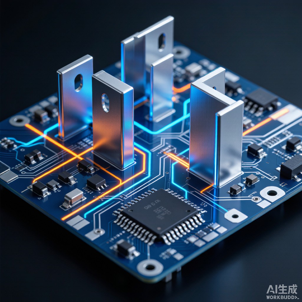
Mixed-signal printed circuit boards combine sensitive analog front-ends, high-speed digital logic, and RF transceivers on a single substrate. The challenge is not simply placing components far apart; at gigahertz frequencies, return currents, power-plane resonances, and magnetic coupling can transmit noise across seemingly isolated regions. Board-level EMI shielding partition walls—raised metal barriers soldered or clipped to the PCB—provide a practical way to compartmentalize noise sources and victims without adding costly enclosure-level shielding. This article explains the coupling mechanisms, wall construction options, layout strategies, and grounding practices that make partition walls effective in SMT assemblies.
How Noise Couples in Mixed-Signal PCBs
Electromagnetic interference in mixed-signal boards travels through several paths:
- Shared impedance coupling: Digital switching currents flowing through a common ground or power plane create voltage drops that modulate analog references.
- Capacitive coupling: Fast voltage transitions on digital traces induce displacement currents in adjacent analog traces.
- Inductive coupling: Time-varying magnetic fields from switching regulators or clock lines couple into sensitive loops.
- Power-plane resonance: Plane pairs form cavity resonators that can radiate or guide noise across the board at specific frequencies.
Traditional mitigation includes careful stack-up design, decoupling capacitors, and trace routing discipline. When these are insufficient—especially in compact IoT, automotive, or medical devices—partition walls add a physical barrier that interrupts electric-field coupling and redirects high-frequency currents.
What Are Board-Level Shielding Partition Walls?
A partition wall is a thin metal fence, typically 0.15–0.50 mm thick and 2–10 mm tall, mounted vertically on the PCB to divide the board into separate electromagnetic zones. Unlike a full shield can that covers an entire component, a partition wall is open at the top, making it compatible with airflow, tall components, and visual inspection. It is often used to:
- Separate RF transceivers from digital processors.
- Isolate power converters from sensitive ADCs.
- Guard high-impedance sensor inputs from switching noise.
- Create clean/dirty ground boundaries along a defined line.
Material Selection and Height Design
Partition walls are stamped or etched from conductive sheet metal and finished with a solderable or conductive-adhesive-compatible coating.
| Material | Relative Permeability | Conductivity (%IACS) | Typical Finish | Application |
|---|---|---|---|---|
| Tin-Plated Steel | ≈100–6,000 | 10–15 | Sn or Sn-Bi | Low-cost magnetic field shielding |
| Brass C2680 | ≈1 | 26–28 | Sn, Ni, or Ag | General electric-field partitions |
| Nickel Silver C7521 | ≈1 | 5–6 | Sn or Ni | Corrosion-resistant, solderable |
| Beryllium Copper | ≈1 | 18–22 | Sn or Ni | Clip-in/resilient partitions |
Wall height is a compromise. Taller walls improve isolation but interfere with component placement and cooling airflow. For electric-field dominated coupling, a height three to five times the wall-to-trace spacing is usually sufficient. For magnetic fields, the wall must form a closed loop with a ground return path; a simple open fence provides limited magnetic shielding.
Layout Placement Strategies
Effective partitioning starts during schematic and floor-pla
ing, not after routing is complete.
Define Zones Early
Group circuits into noise domains: RF, digital, analog, and power. Place partition walls along the boundaries of these domains. Critical high-impedance nodes should be located farthest from switching sources, with the wall placed between them.
Keep Traces Perpendicular to the Wall
When a trace must cross a partition boundary, route it perpendicular to the wall at the crossing point. This minimizes the coupled length and keeps the return current path predictable. Avoid ru
ing high-speed traces parallel to a wall on the victim side.
Maintain Clearance Around Vias and Components
Wall placement must respect component keep-out zones, solder mask dams, and test probe access. A typical clearance is 0.5–1.0 mm from SMT pads and 1.0–2.0 mm from tall components. Slots or notches in the wall accommodate unavoidable trace crossings while preserving most of the barrier.
Grounding and Via Fencing
A partition wall is only as effective as its grounding. An ungrounded metal fence can become a resonant ante
a rather than a shield. Best practices include:
- Continuous ground stitch: Solder the wall to a solid ground trace or plane edge at intervals of λ/20 or less at the highest frequency of concern. For 2.4 GHz, this is roughly 6 mm.
- Via fencing: Place a row of grounded vias, typically 0.3–0.5 mm diameter on 1.0 mm pitch, immediately beneath the wall footprint. The via barrel co
ects the top and bottom ground planes, reducing edge radiation.
- Single-point co
ection of analog and digital grounds:
If the wall separates analog and digital zones, coect their respective ground planes at one controlled location, often under or near an ADC/DAC.
- Avoid ground loops: Do not create multiple parallel ground paths across the partition; this invites circulating currents.
Design Checklist
Before releasing a mixed-signal PCB with partition walls, verify the following:
- Have all noise sources and sensitive circuits been grouped into separate zones?
- Is the partition wall grounded at intervals appropriate for the highest operating frequency?
- Are via fences placed directly beneath the wall path?
- Have traces crossing the boundary been routed perpendicular to the wall?
- Does the wall material match the soldering or adhesive process (reflow, wave, conductive epoxy)?
- Have mechanical clearances been checked against component heights and pick-and-place nozzles?
- Is the wall open geometry compatible with required airflow and thermal paths?
Conclusion
Board-level EMI shielding partition walls are a cost-effective, compact method for isolating noise domains on mixed-signal PCBs. Success depends on early zoning, proper material selection, tight grounding, and disciplined trace routing at partition crossings. When combined with good stack-up and decoupling design, partition walls can reduce crosstalk and radiated emissions by 10–30 dB, helping compact electronic products meet EMC targets without heavy full-metal enclosures.



