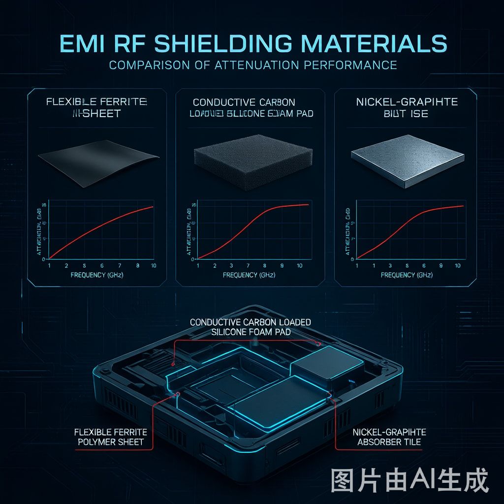
Introduction: The Near-Field EMI Challenge in Compact IoT Devices
As IoT devices shrink to ever smaller form factors — smart sensors, wearable trackers, wireless beacons, and edge computing nodes — the electromagnetic interference (EMI) challenge shifts from far-field shielding (preventing external RF penetration) to near-field suppression (containing internal ante
a-to-circuit coupling). In a 30 mm × 30 mm IoT module, the Bluetooth/Wi-Fi ante
a sits within 2–5 mm of the digital processor, power management IC, and sensor front-end, creating intense near-field magnetic coupling that desenses the receiver and degrades link budget by 5–15 dB.
Traditional EMI shielding cans (metal enclosures) reflect rather than absorb electromagnetic energy, potentially worsening near-field coupling through cavity resonance effects. Absorber materials — which convert EM energy into heat through magnetic or dielectric loss mechanisms — provide a more effective solution for near-field suppression. This article compares three dominant absorber material classes for IoT device applications.
Absorber Material Physics: Absorption vs Reflection
How Absorbers Work
EMI absorber materials attenuate electromagnetic waves through three mechanisms:
– Magnetic loss: Ferrite particles (MnZn, NiZn) exhibit complex permeability μ = μ’ — jμ”, where μ” (imaginary permeability) represents energy dissipation through domain wall resonance and spin resonance.
– Dielectric loss: Carbon and conductive fillers create complex permittivity ε = ε’ — jε”, where ε” represents energy conversion through interfacial polarization (Maxwell-Wagner effect) and conduction loss.
– Impedance matching: The absorber’s intrinsic impedance Z = √(μ/ε) should approximate free-space impedance Z₀ = 377 Ω to minimize reflection at the absorber surface — more energy enters the absorber rather than bouncing back.
The absorption effectiveness is measured as insertion loss (IL) in dB, comprising both reflection loss (RL) and absorption loss (AL): IL = RL + AL. An ideal absorber maximizes AL and minimizes RL.
Material Class 1: Flexible Ferrite Polymer Sheet
Composition and Performance
Flexible ferrite polymer sheets consist of NiZn ferrite powder (70–85% volume loading) dispersed in a silicone or polyurethane binder matrix, formed into thin sheets (0.1–1.0 mm thickness). The ferrite provides magnetic loss, while the polymer matrix maintains flexibility and conformability.
| Parameter | Typical Range | Notes |
|---|---|---|
| Ferrite loading | 70–85 vol% | NiZn ferrite preferred for >100 MHz |
| Sheet thickness | 0.1–1.0 mm | 0.2–0.5 mm typical for IoT |
| μ’ at 100 MHz | 8–15 | Real permeability (energy storage) |
| μ” at 100 MHz | 3–8 | Imaginary permeability (energy loss) |
| IL at 2.4 GHz (0.3mm) | 5–12 dB | Bluetooth band, single-layer |
| IL at 5.8 GHz (0.3mm) | 10–20 dB | Wi-Fi 6 / 5G sub-6GHz |
| Flexibility | Conformable | Bend radius ≥5 mm |
| Operating temperature | —40 to +150°C | Silicone binder |
| Weight (0.3mm sheet) | 1.5–2.5 g/cm² | Relatively heavy |
Advantages for IoT: High absorption at 2.4/5.8 GHz (the primary IoT wireless bands), conformable to curved device surfaces, thin profile fits tight packaging constraints, temperature-stable performance.
Limitations: Heavy relative to other absorbers (density 3.5–4.5 g/cm³), ferrite loading makes sheet somewhat stiff (bend radius >5 mm required), single-layer absorption limited to ~12 dB at 2.4 GHz — multi-layer stacking needed for >15 dB.
Material Class 2: Conductive Carbon Foam
Composition and Performance
Conductive carbon foam (also called carbon-loaded foam or RF absorber foam) consists of a reticulated polyurethane or melamine foam substrate (3–6 mm thickness) impregnated with carbon black or graphite particles, coated with a conductive carbon ink layer. This creates a gradient impedance structure that progressively absorbs EM energy through the foam thickness.
| Parameter | Typical Range | Notes |
|---|---|---|
| Foam thickness | 3–6 mm | Thicker = more absorption |
| Carbon loading | 5–15 wt% | Gradient distribution optimal |
| ε’ at 2.4 GHz | 4–12 | Real permittivity |
| ε” at 2.4 GHz | 2–8 | Imaginary permittivity (loss) |
| IL at 2.4 GHz (6mm) | 15–25 dB | Excellent broadband absorption |
| IL at 5.8 GHz (6mm) | 20–30 dB | Higher frequency = better |
| IL at 100 MHz | 3–8 dB | Weaker at low frequencies |
| Density | 0.08–0.15 g/cm³ | Very lightweight |
| Operating temperature | —20 to +80°C | Polyurethane limited |
Advantages for IoT: Extremely lightweight (density 0.08–0.15 g/cm³), broadband absorption (excellent above 1 GHz), gradient impedance reduces reflection, thick profile provides high IL in a single piece.
Limitations: Minimum 3 mm thickness required (space constraint in ultra-compact IoT), weak absorption below 500 MHz (not suitable for NFC/RFID near-field), polyurethane substrate temperature-limited to 80°C, foam compressibility means mechanical design must prevent crushing.
Material Class 3: Carbon-Loaded Silicone Rubber
Composition and Performance
Carbon-loaded silicone rubber sheets consist of carbon black or nickel-graphite particles dispersed in silicone rubber matrix, formed into sheets (0.5–2.0 mm). This material combines dielectric loss (from carbon) with moderate conductivity (for surface reflection suppression) and silicone’s inherent flexibility and temperature resistance.
| Parameter | Typical Range | Notes |
|---|---|---|
| Sheet thickness | 0.5–2.0 mm | 1.0 mm typical for IoT |
| Carbon/nickel loading | 15–30 vol% | Nickel-graphite for higher loss |
| ε’ at 2.4 GHz | 10–25 | High real permittivity |
| ε” at 2.4 GHz | 5–15 | Strong dielectric loss |
| IL at 2.4 GHz (1mm) | 8–15 dB | Moderate absorption |
| IL at 5.8 GHz (1mm) | 12–18 dB | Better at higher frequency |
| Surface resistivity | 10–100 Ω/sq | Also provides reflection shielding |
| Density | 1.5–2.5 g/cm³ | Medium weight |
| Operating temperature | —40 to +200°C | Silicone excellent temp range |
| Flexibility | Highly conformable | Bend radius ≥3 mm |
Advantages for IoT: Dual function (absorption + surface shielding), thin profile (0.5 mm minimum), highly conformable, excellent temperature range, good absorption at IoT frequencies.
Limitations: High permittivity creates impedance mismatch → significant reflection component (not pure absorber), denser than carbon foam, absorption per-unit-thickness lower than ferrite sheet at 2.4 GHz.
Comparative Selection Guide for IoT Device Applications
| Selection Criterion | Ferrite Sheet | Carbon Foam | Carbon Silicone |
|---|---|---|---|
| Space available < 1mm | ★★★★★ (0.1mm min) | ★☆☆☆☆ (3mm min) | ★★★★☆ (0.5mm min) |
| Space available 3–6mm | ★★★☆☆ | ★★★★★ (best IL) | ★★★☆☆ |
| 2.4 GHz absorption priority | ★★★★☆ | ★★★★★ | ★★★☆☆ |
| Broadband 1–6 GHz | ★★★☆☆ | ★★★★★ | ★★★☆☆ |
| NFC/RFID < 100 MHz | ★★★★★ | ★☆☆☆☆ | ★★☆☆☆ |
| Weight-critical (wearable) | ★★☆☆☆ | ★★★★★ | ★★★☆☆ |
| Conformability (curved surface) | ★★★☆☆ | ★★★★☆ | ★★★★★ |
| Temperature >100°C | ★★★★★ | ★☆☆☆☆ | ★★★★★ |
| Dual shielding + absorption | ★☆☆☆☆ | ★☆☆☆☆ | ★★★★★ |
Recommended selection strategy:
– Ultra-thin IoT (phone, wearable): Ferrite sheet 0.2–0.3 mm — only option fitting <1mm space
– Standard IoT module (30×30mm+): Carbon foam 4–6 mm — best IL per volume, lightweight
– Harsh environment IoT (industrial, automotive): Carbon-loaded silicone 1.0 mm — best temperature + dual function
– NFC/RFID-enabled IoT: Ferrite sheet — only material with effective absorption below 100 MHz
Practical Implementation Considerations
Placement Strategy
Absorber material should be placed between the ante
a element and the noise-generating circuit block, not wrapped around the ante
a (which would attenuate the desired signal). For a typical IoT PCB layout:
– Place absorber sheet on the PCB surface facing the ante
a (circuit side)
– Maintain 2–3 mm air gap between absorber and ante
a for desired signal propagation
– Cut absorber to cover only the digital/power section, not the RF section
– Avoid covering ante
a ground plane edge (critical for ante
a efficiency)
Adhesive Selection
– 3M 467MP transfer adhesive: Standard for ferrite and silicone absorber attachment, 0.05 mm thickness, 150°C service temperature
– Double-coated PET tape: For foam absorber, prevents adhesive wicking into foam structure
– Thermal adhesive pad: When absorber also serves as thermal interface for power device heat spreading
Conclusion
EMI absorber material selection for IoT device near-field suppression depends on three primary constraints: available space, target frequency band, and environmental conditions. Ferrite polymer sheets dominate ultra-thin (<1 mm) and low-frequency applications, carbon foam provides the best broadband absorption in 3–6 mm space, and carbon-loaded silicone offers dual shielding-absorption function with superior temperature resistance. Strategic placement between ante
a and noise sources, rather than around the ante
a, preserves desired signal integrity while suppressing parasitic near-field coupling — a critical design principle for maintaining IoT wireless link budget in compact form factors.



