What Is Electrochemical Migration?
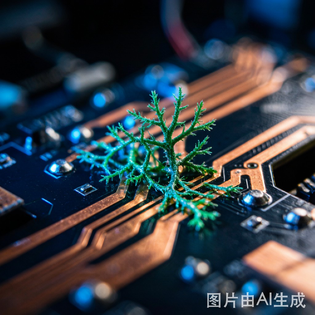
Electrochemical migration (ECM) is a failure mechanism in which dissolved metal ions migrate across a printed circuit board (PCB) surface under the influence of an electric field, redepositing as metallic dendrites that bridge adjacent conductors. On bare copper traces, the anode dissolves into Cu²⁺ ions that travel through a thin electrolyte film toward the cathode, forming tree-like conductive structures that cause short circuits, leakage currents, and intermittent failures.
For manufacturers and assemblers in Southeast Asia, ECM is particularly relevant because the combination of high ambient humidity (>75% RH), elevated temperatures, and residual ionic contamination from flux residues creates ideal conditions for dendritic growth. A 0.5 mm gap between copper pads can develop a bridging dendrite in as little as 72 hours under 85°C/85% RH bias testing.
Root Causes and Contributing Factors
Ionic Contamination Residues
The most common trigger for ECM is residual ionic contamination from no-clean flux activators, solder paste residues, or handling contamination. Halide-based activators (chloride, bromide) are especially problematic because they lower the electrochemical potential required for copper dissolution. Even “no-clean” formulations leave hygroscopic residues that absorb atmospheric moisture and form conductive electrolyte films.
Humidity and Temperature Acceleration
Water vapor condensation on PCB surfaces provides the electrolyte necessary for ion migration. The Arrhenius relationship shows that ECM rates approximately double for every 10°C increase above 25°C. In tropical climates where warehouses and assembly floors may experience 30–35°C with 80–90% RH, unprotected copper surfaces are at significant risk.
Voltage Gradient and Gap Spacing
ECM is driven by the electric field between biased conductors. Higher voltage gradients accelerate ion transport, while smaller gaps reduce the time-to-failure. IPC research indicates that reducing conductor spacing from 0.5 mm to 0.3 mm at 5 V DC bias can reduce the mean time to failure by 40–60% on contaminated surfaces.
Testing and Detection Methods
IPC-TM-650 Method 2.6.14 (Electrochemical Migration Resistance Test) is the industry-standard accelerated life test. Samples are subjected to 65°C/85% RH with a DC bias voltage (typically 10–50 V) while insulation resistance is monitored. A resistance drop below 10⁸ ohms indicates dendritic bridging.
Complementary detection methods include:
- Surface Insulation Resistance (SIR) testing per IPC-TM-650 2.6.3.3 for real-time monitoring during assembly qualification
- Ionic contamination (ROSE) testing per IPC-TM-650 2.3.25 to quantify residual ionic levels before and after cleaning
- Optical microscopy and SEM imaging for post-failure dendrite morphology analysis
- Electrochemical impedance spectroscopy (EIS) for early-stage corrosion film characterization
Prevention and Mitigation Strategies
Material Selection
Select halide-free solder pastes and fluxes with low ionic activator content. For bare copper applications, consider immersion tin or OSP surface finishes that provide a thin barrier layer without significantly affecting solderability. For high-reliability applications, ENIG or ENEPIG finishes eliminate exposed copper entirely.
Process Control
Maintain ROSE values below 1.56 μg NaCl-equivalent/cm² per IPC J-STD-001. Implement deionized (DI) water washing after soldering for no-clean processes that must meet Class 3 reliability. Ensure complete drying after cleaning—residual water films are more dangerous than controlled ionic residues.
Conformal Coating and Encapsulation
Acrylic, polyurethane, or silicone conformal coatings create a moisture barrier that suppresses ECM by preventing water film formation. For severe environments, epoxy potting or parylene deposition provides complete encapsulation. Coating thickness of 25–75 μm is typically sufficient; verify coverage with UV fluorescence inspection for acrylics.
Design-for-Reliability Guidelines
Increase conductor spacing in high-voltage or high-humidity zones. Avoid sharp trace corners that create localized field concentration. Route high-voltage traces away from ground planes with minimum insulation gaps. Use guard rings around sensitive analog circuits to intercept migrating ions before they reach critical nodes.
Galvanic Corrosion in Mixed-Metal Assemblies
A related failure mode is galvanic corrosion, which occurs when dissimilar metals (e.g., copper and aluminum, or copper and tin-coated steel) are in electrical contact in the presence of an electrolyte. The galvanic series dictates that copper (noble potential +0.34 V SHE) will act as the cathode while less noble metals corrode preferentially. In SMT assemblies with nickel-plated copper lead frames and tin-silver-copper solder, the primary risk is localized corrosion at the solder joint interface, accelerating creep failure under mechanical or thermal stress.
Mitigation includes nickel barrier layers between copper and tin, conformal coating over mixed-metal interfaces, and avoiding aluminum hardware or heatsinks in direct contact with bare copper traces without insulating washers or thermal interface materials.
Conclusion
Electrochemical migration and galvanic corrosion represent significant reliability risks for copper-based PCBs and SMT assemblies in tropical and humid environments. A layered defense combining low-residue materials, rigorous ionic cleanliness, conformal coating, and design-for-reliability spacing is essential. For manufacturers in Southeast Asia, integrating ECM testing into new product qualification and maintaining controlled assembly environments can prevent costly field failures and protect brand reputation.



