Introduction
Copper wire bonding has become the dominant interco
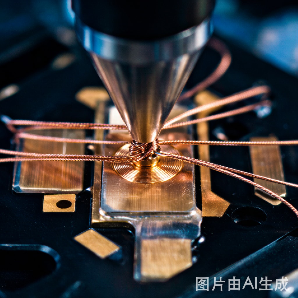
ection technology in power semiconductor packaging, displacing aluminum wire in applications demanding higher current density, better thermal performance, and improved reliability. Wedge bonding — where ultrasonic energy is applied through a wedge-shaped tool to bond a free-air copper wire to the bond pad — is the preferred method for power packages due to its ability to handle large wire diameters (200-500 µm) and produce low-profile, high-reliability bonds. Optimizing this process requires a systematic understanding of the interdependent ultrasonic, thermal, and mechanical parameters.
Ultrasonic Wedge Bonding Fundamentals
Wedge bonding creates a metallurgical bond through the simultaneous application of ultrasonic energy and normal force. The ultrasonic transducer oscillates the wedge tool at 60-120 kHz with an amplitude of 1-5 µm, scrubbing the copper wire against the bond pad surface. This scrubbing action:
- Removes surface oxides and contaminants: The mechanical scrubbing action displaces native oxides (Cu₂O on copper pads, Al₂O₃ on aluminum pads) and adsorbed contamination layers, exposing clean metal surfaces.
- Promotes atomic diffusion: The combination of localized heating from friction and intimate atomic contact enables interdiffusion across the bond interface, forming a solid-state weld.
- Deforms the copper wire: The applied normal force (typically 200-800 gf for 300 µm wire) flattens the wire against the pad, increasing the bonded area and mechanical strength.
Key Process Parameters
Successful copper wedge bonding requires precise control of multiple interacting parameters:
| Parameter | Typical Range (300 µm Cu Wire) | Effect |
|---|---|---|
| Ultrasonic Power | 0.5-2.0 W | Higher power increases scrub amplitude, improving oxide removal and diffusion. Excessive power causes wire cracking or pad cratering. |
| Bond Force (Normal) | 300-600 gf | Controls wire deformation (target: 130-180% of original wire diameter in bond width). Excessive force damages the die metallization. |
| Bond Time | 20-100 ms | Longer time increases bond strength asymptotically. Beyond optimal time, work hardening and fatigue damage accumulate. |
| Stage Temperature | 150-250°C | Elevated temperature enhances diffusion kinetics and softens metals. Copper requires higher temperature than aluminum (120-180°C) due to its higher hardness. |
| Ultrasonic Frequency | 60-100 kHz | Higher frequency produces finer scrubbing action, beneficial for thin bond pad metallization. Lower frequency provides more aggressive oxide removal. |
Bond Pad Metallization for Copper Wire
Copper wire is harder than gold or aluminum wire, imposing stricter requirements on bond pad metallization. The pad structure must absorb ultrasonic energy without cracking the underlying silicon or dielectric layers:
- Aluminum pad (2-4 µm): The most common metallization for power devices. Copper wire bonds well to aluminum pads at elevated temperature (220-250°C), forming Cu-Al intermetallics. However, Cu-Al IMC growth under high-temperature operation can create Kirkendall voids, requiring nickel or palladium diffusion barriers.
- Nickel-palladium-gold pad: An increasingly common pad stack for copper wire. The thin gold flash (0.05-0.1 µm) protects the nickel surface, the palladium layer (0.1-0.3 µm) provides oxidation resistance, and the underlying nickel (1-3 µm) acts as a mechanical buffer for the hard copper wire. This pad structure eliminates Cu-Al IMC reliability concerns.
- Copper pad (bare or silver-plated): For the ultimate in homogeneous bonding, copper wire on copper pads produces Cu-Cu bonds with no intermetallic formation concerns. Silver-plated copper pads improve bondability without introducing dissimilar metals.
Wedge Tool Geometry and Material
The wedge tool is a consumable precision component whose geometry directly influences bond quality. Key geometric parameters include:
- Hole diameter: Must match the wire diameter with 5-10% clearance. Excessive clearance allows wire wandering during bonding; insufficient clearance causes wire jamming and feed inconsistency.
- Foot length: Determines the bonded area. Typical foot length is 1.5-2.5× the wire diameter. Longer feet produce stronger bonds but increase the risk of tail bond and require more space on the bond pad.
- Feed angle: The angle at which wire exits the tool. Typically 30° or 45°. The feed angle affects wire looping characteristics and the formation of the second bond (stitch bond) on the lead frame.
- Tool material: Tungsten carbide (WC) is standard for copper wire bonding. Ceramic tools (alumina or zirconia-toughened alumina) offer longer life when bonding on hard pad metallizations like nickel.
Process Window Development
Developing a robust process window requires design of experiments (DOE) methodology. A typical approach varies ultrasonic power, bond force, and bond time in a three-factor central composite design, measuring bond shear strength and visual quality as responses. The process window is defined by:
- Lower bound: Minimum shear strength per MIL-STD-883 Method 2011.9 (typically ≥5 gf/mil² or ≥25 gf for a 300 µm wire).
- Upper bound: Maximum acceptable pad damage — no visible cratering at 100× magnification, and no cracks exceeding 10% of pad thickness in cross-section.
- Optimal center: Highest shear strength with minimal standard deviation, representing the most robust operating point for production variability.
Reliability Testing
Copper wire bonds in power packages must survive harsh reliability testing:
- High Temperature Storage (HTS): 1,000 hours at 175-200°C. Measures IMC growth kinetics and bond resistance drift. Copper wire on NiPdAu pads typically shows <5% resistance increase; Cu-Al bonds may show 10-20% increase due to IMC consumption.
- Temperature Cycling (TC): -55°C to +150°C, 1,000-2,000 cycles. Evaluates thermomechanical fatigue caused by CTE mismatch between the copper wire, bond pad, and mold compound.
- Power Cycling (PC): ΔTj = 100-150°C, 50,000-100,000 cycles. The ultimate reliability test for power packages, combining thermal and electrical stress. Copper wire consistently outperforms aluminum in power cycling due to its higher melting point and superior fatigue resistance.
Conclusion
Copper wire wedge bonding for SMT power packages requires precise control of ultrasonic energy, bond force, temperature, and bond pad metallization. The transition from aluminum to copper wire delivers measurable improvements in current density, thermal performance, and power cycling reliability — benefits that are essential for next-generation SiC and GaN power modules. By systematically optimizing process parameters and selecting appropriate bond pad metallization stacks (NiPdAu or silver-plated copper), manufacturers can achieve robust, high-yield copper wire bonding processes that meet the demanding reliability requirements of automotive, industrial, and renewable energy applications.



