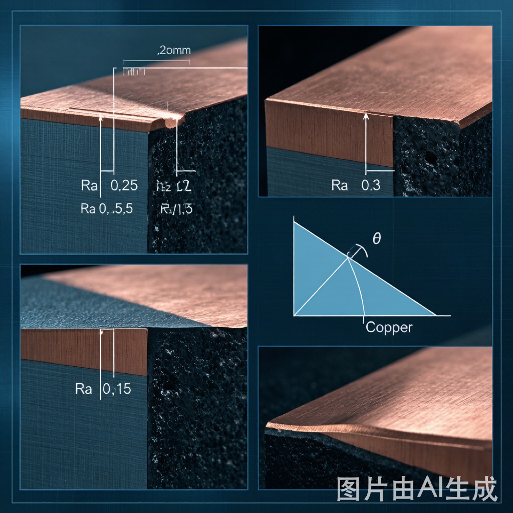
Why Surface Roughness Matters for SMT Solder Joints
The surface roughness of copper strip used in SMT component manufacturing is a critical but often under-specified parameter that directly affects solder wetting behavior, joint formation, and long-term reliability. While most procurement specifications focus on dimensional accuracy (thickness, width, flatness), the micro-scale surface texture—measured as Ra (arithmetic average roughness), Rz (maximum peak-to-valley height), and Rmax (maximum roughness depth)—determines how solder interacts with the copper surface during reflow.
Solder wetting is governed by surface energy interactions at the liquid solder-solid copper interface. The contact angle between molten solder and copper is a direct measure of wettability—and this contact angle is profoundly influenced by surface roughness through well-established physical models. Understanding and controlling copper strip surface roughness is essential for achieving consistent, reliable solder joints in SMT assembly.
Surface Roughness Parameters: Ra, Rz, and Rmax
Ra (Arithmetic Average Roughness)
Ra is the most commonly specified surface roughness parameter. It represents the arithmetic mean of the absolute values of the profile deviations from the mean line over a sampling length. For copper strip used in SMT applications, typical Ra values range from 0.1 to 1.5 micrometers, depending on the manufacturing process:
- Cold-rolled strip: Ra 0.1-0.4 micrometers (smooth, mirror-like)
- Hot-rolled strip: Ra 0.5-1.5 micrometers (rougher, matte finish)
- Mechanically polished strip: Ra 0.05-0.15 micrometers (very smooth)
- Electrodeposited strip: Ra 0.2-0.8 micrometers (moderate, with nodular texture)
Rz (Maximum Peak-to-Valley Height)
Rz is the average of the maximum peak-to-valley heights within five sampling lengths. Rz is more sensitive to extreme surface features (deep scratches, pits) than Ra, making it a better indicator of surface defects that could trap contaminants or create localized wetting failures. For SMT-grade copper strip, Rz is typically 4-6 times the Ra value.
Rmax (Maximum Roughness Depth)
Rmax is the single largest peak-to-valley height within the evaluation length. This parameter identifies the worst-case surface feature—a deep scratch or pit that could act as a stress concentrator or contamination trap. Rmax is particularly important for fatigue-critical applications where surface defects can initiate crack propagation.
Measurement Standards and Methods
Surface roughness is measured per ISO 4287 (profile-based parameters) using either contact (stylus) or non-contact (optical) profilometry:
- Stylus profilometer (contact): A diamond-tipped stylus (2-5 micrometers tip radius) traverses the surface at 0.5 mm/s, recording the vertical displacement. Resolution: 0.01 micrometers. This is the standard method for production line inspection and incoming QC. Measurement cost: $0 (in-house) to $5-10 per sample (lab).
- Optical profilometer (non-contact): White-light interferometry or laser confocal sca
ing provides a 3D surface map without contacting the surface. Resolution: 0.001 micrometers. This method captures areal parameters (Sa, Sz) in addition to profile parameters. Preferred for research and development applications. Equipment cost: $30,000-80,000.
- Atomic Force Microscopy (AFM): For nanoscale surface characterization (Ra < 0.01 micrometers). Used in research settings to study the effect of nano-scale texture on wetting behavior. Not practical for production QC.
The Physics of Solder Wetting on Rough Surfaces
Young’s Equation and Contact Angle
The fundamental relationship governing solder wetting is Young’s equation: cos(theta) = (gamma_sv – gamma_sl) / gamma_lv, where theta is the contact angle, gamma_sv is the solid-vapor surface energy, gamma_sl is the solid-liquid interfacial energy, and gamma_lv is the liquid-vapor surface tension. For molten SAC305 solder on clean copper, the intrinsic (Young’s) contact angle is 15-25 degrees—indicating excellent wetting.
Wenzel Model: Roughness Amplifies Wetting
The Wenzel model describes how surface roughness modifies the apparent contact angle: cos(theta_w) = r * cos(theta_y), where r is the roughness ratio (actual surface area / projected surface area, always >= 1) and theta_y is Young’s intrinsic contact angle. For copper with solder, where theta_y < 90 degrees (wetting is favorable), increasing roughness decreases the apparent contact angle—improving wetting. This is because roughness increases the effective contact area, amplifying the surface energy effect.
Practical implication: Moderate surface roughness (Ra 0.3-0.8 micrometers) improves solder wetting compared to perfectly smooth copper (Ra 0.05 micrometers). The roughness provides micro-scale mechanical interlocking sites and increases the effective surface energy contact area.
Cassie-Baxter Model: Roughness Can Hinder Wetting
However, when surface roughness creates deep valleys that trap air or contaminants, the Cassie-Baxter model applies instead: the molten solder sits on top of the peaks without penetrating the valleys, creating a “composite” surface of solder-air and solder-copper interfaces. This produces a high apparent contact angle (>90 degrees) and poor wetting, even though the intrinsic copper-solder chemistry is favorable.
Practical implication: Excessive roughness (Ra > 1.5 micrometers) with deep, narrow valleys (valley aspect ratio > 1:1) can trap flux residues, oxidation products, or air pockets that prevent solder penetration, degrading wetting despite the favorable Wenzel effect.
Optimal Roughness Range for SMT Soldering
| Ra Range (um) | Surface Character | Wetting Quality | Joint Reliability | Recommendation |
|---|---|---|---|---|
| 0.05-0.15 | Very smooth (polished) | Good but slow | Fair (low mechanical bond) | Not recommended |
| 0.15-0.30 | Smooth (cold-rolled) | Good | Good | Acceptable for ENIG/ENEPIG |
| 0.30-0.60 | Medium (optimal) | Excellent | Excellent | Recommended for bare copper |
| 0.60-1.00 | Rough (hot-rolled) | Good (with active flux) | Good | Acceptable with RA flux |
| 1.00-1.50 | Very rough | Fair (valley trapping) | Fair (stress concentration) | Not recommended |
| > 1.50 | Excessively rough | Poor (Cassie-Baxter) | Poor (crack initiation) | Reject |
Contact Angle Measurement for Wetting Assessment
The solder contact angle on copper can be measured directly using a wetting balance tester or a sessile drop method:
Wetting Balance Test
Per J-STD-002, a copper test coupon is immersed in molten SAC305 at 245 degrees C with RMA flux. The wetting force is measured over time, and the contact angle is calculated from the equilibrium wetting force. Typical contact angles for different Ra values:
- Ra 0.10 micrometers: Contact angle 28-35 degrees
- Ra 0.40 micrometers: Contact angle 15-22 degrees (optimal)
- Ra 0.80 micrometers: Contact angle 18-25 degrees
- Ra 1.50 micrometers: Contact angle 35-50 degrees (degraded)
Sessile Drop Method
Place a 0.3 mm SAC305 solder sphere on the copper surface, apply flux, and heat on a hot plate at 250 degrees C until the sphere melts and wets the surface. After solidification, cross-section the sample and measure the contact angle under a microscope. This method provides a direct visual measurement of the wetting geometry and is useful for comparing different surface finishes.
Impact of Roughness on Joint Reliability
Mechanical Bond Strength
Moderate surface roughness (Ra 0.3-0.6 micrometers) improves mechanical bond strength through micro-interlocking between the solder and the copper surface asperities. The solder flows into the micro-scale valleys and, upon solidification, forms mechanical anchors that resist shear and peel forces. Shear strength testing of solder joints on copper with Ra 0.4 micrometers shows 10-20% higher shear force compared to joints on polished copper (Ra 0.1 micrometers).
However, excessive roughness (Ra > 1.0 micrometers) creates stress concentration points at the valley roots. Under thermal cycling, these stress concentrations can initiate micro-cracks in the solder joint, reducing fatigue life by 30-50% compared to optimally rough surfaces.
Intermetallic Compound Formation
Surface roughness affects the uniformity of the Cu6Sn5 intermetallic layer that forms during reflow. On smooth surfaces (Ra 0.8 micrometers), the IMC thickness varies significantly across peaks and valleys—thicker at the peaks (where solder contact is longer) and thi
er or absent in the valleys (where flux residues may prevent contact). This non-uniform IMC creates weak spots in the joint that fail preferentially under mechanical stress.
Void Formation
Rough surfaces trap more volatiles (flux solvents, moisture) in the valleys during reflow. As these volatiles evaporate during the reflow cycle, they create voids in the solder joint. Void content in joints on Ra 0.4 micrometers copper is typically 3-8%, while void content on Ra 1.2 micrometers copper can reach 12-20%. IPC-A-610 limits voiding to 25% (Class 2) or 10% (Class 3), so excessive roughness can push voiding beyond acceptance limits.
Process Controls for Consistent Surface Roughness
Incoming Inspection
Specify surface roughness requirements in copper strip purchase orders: “Ra 0.3-0.6 micrometers, Rz 5.0 micrometers (indicating deep scratches).
Manufacturing Process Control
The surface roughness of copper strip is primarily determined by the cold rolling process—specifically the roll surface finish, rolling reduction, and lubrication. To maintain consistent roughness:
- Roll surface specification: Specify the work roll surface finish as Ra 0.1-0.2 micrometers (ground finish). The roll finish transfers to the strip surface during rolling.
- Lubrication control: Rolling oil viscosity and flow rate affect the strip surface finish. Use synthetic rolling oil with viscosity 5-10 cSt at 40 degrees C, applied at 2-5 L/min per roll.
- Reduction rate: Higher reduction rates (>50% per pass) produce smoother surfaces but increase work hardening. Balance reduction rate with intermediate a
ealing to maintain both surface finish and mechanical properties.
Post-Processing Surface Treatment
If incoming copper strip roughness is outside specification, surface treatment can adjust it:
- Mechanical polishing (to reduce roughness): Belt grinding with 400-600 grit abrasive reduces Ra from 0.8-1.2 micrometers to 0.2-0.4 micrometers. Suitable for batch processing but adds 5-10% material loss.
- Chemical etching (to increase roughness): Immersion in dilute FeCl3 or CuCl2 solution (5-10% concentration, 10-30 seconds) micro-etches the surface, increasing Ra from 0.1 to 0.3-0.5 micrometers. This is the preferred method for preparing smooth cold-rolled strip for SMT applications.
- Electroplating (to modify surface): Electroless nickel or copper plating creates a new surface layer with controlled roughness. This is used when both surface finish and roughness need modification.
Conclusion
Copper strip surface roughness is a critical parameter that directly affects solder wetting behavior, mechanical bond strength, intermetallic compound uniformity, and void content in SMT solder joints. The optimal Ra range for SMT applications is 0.3-0.6 micrometers—rough enough to provide micro-mechanical interlocking and amplify wetting via the Wenzel effect, but smooth enough to avoid valley trapping of volatiles and stress concentration. Surface roughness should be specified in procurement documents, measured during incoming inspection, and controlled through rolling process parameters. When roughness is outside specification, chemical etching or mechanical polishing can adjust it to the optimal range. By treating surface roughness as a first-class quality parameter alongside dimensional accuracy, SMT manufacturers can achieve more consistent solder joint quality and higher long-term reliability in their assemblies.



