## Introduction
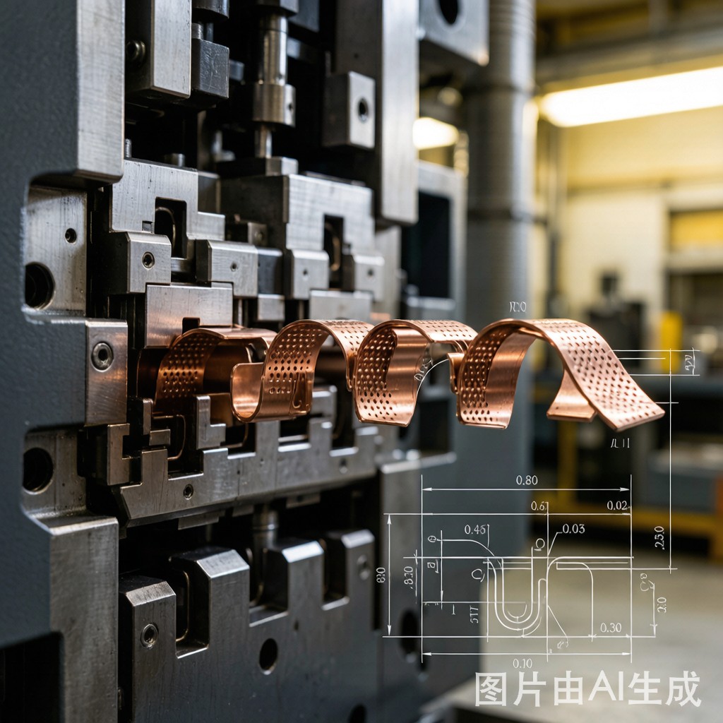
Battery contact springs manufactured from copper alloy strip are ubiquitous in SMT (Surface Mount Technology) electronics — from CR2032 coin cell retainers on IoT boards to multi-cell contact arrays in portable medical devices. The punching and perforation processes that transform flat strip into functional spring contacts demand precision die design, alloy-specific process parameters, and rigorous burr control that directly impact spring force consistency, solder joint reliability, and long-term contact stability.
This article examines the technical chain from alloy selection through progressive die punching, perforation pattern design, and quality verification for SMT battery contact spring manufacturing.
## Alloy Selection for Battery Contact Springs
### Phosphor Bronze C52100 (R-H02 Temper)
C52100 (8% Sn, 0.1% P, balance Cu) in half-hard temper (H02) is the dominant alloy for SMT battery contacts due to its combination of spring properties, solderability, and cost efficiency.
| Property | C52100 R-H02 | C52100 R-H04 | C7521 (Ni-Ag) H02 |
|———-|————-|————-|———————|
| Yield Strength | 310 MPa | 520 MPa | 340 MPa |
| Elastic Modulus | 110 GPa | 110 GPa | 130 GPa |
| Springback Angle | 5-8° | 12-18° | 3-5° |
| Conductivity (IACS) | 13% | 13% | 9% |
| Solderability (J-STD-002) | Class 3 | Class 3 | Class 2 |
| Cost Index | 1.0 | 1.0 | 1.8 |
C52100 R-H02 is preferred for standard battery clips where moderate spring force (0.5-2.0 N) is required. R-H04 full-hard temper is specified for high-force contacts (>3.0 N) in industrial and automotive battery holders where permanent set resistance is critical.
C7521 (Nickel Silver, 18% Ni, 17% Zn, balance Cu) offers superior solderability resistance (immune to tin whisker growth) and natural nickel-white appearance but at higher cost and lower conductivity — suited for premium consumer electronics where aesthetic appearance of exposed contacts matters.
### Strip Thickness Selection
Battery contact spring thickness directly determines spring force per unit deflection:
F = E × w × t³ / (4 × L³) (simplified cantilever beam model)
Where E = elastic modulus, w = contact width, t = strip thickness, L = spring arm length.
| Application | Typical Thickness | Spring Force Range | Battery Type |
|————|—————–|——————-|————-|
| Coin cell retainer | 0.15-0.20mm | 0.3-1.0 N | CR2032/CR1220 |
| AAA/AA single contact | 0.20-0.30mm | 1.0-3.0 N | AAA/AA |
| Multi-cell array | 0.25-0.35mm | 2.0-5.0 N | 2-4× AA |
| Industrial high-force | 0.35-0.50mm | 5.0-15.0 N | 18650 Li-Ion |
## Progressive Die Punching Process
### Die Station Sequence
A typical 8-12 station progressive die for battery contact springs processes strip at 200-400 strokes per minute (SPM) with strip advance of 8-15mm per stroke:
| Station | Operation | Critical Parameters |
|———|———–|——————-|
| 1 | Pilot punch + strip alignment | Pilot diameter = pin Ø + 0.01mm |
| 2 | Perforation (mounting holes) | Punch-die clearance = 5-8% × t |
| 3 | Blank / rough form cut | Clearance = 6-10% × t |
| 4 | Bend arm (90° L-form) | Bend radius R = 1.5-2× t (C52100) |
| 5 | Form contact dome / radius | Dome radius = battery radius ± 0.05mm |
| 6 | Spring arm camber (pre-set) | Camber angle = operating deflection × 1.3 |
| 7 | Trim / final cutoff | Trim clearance = 4-6% × t |
| 8 | Idle / carrier strip cutoff | Part separation |
### Punch-Die Clearance Optimization
Clearance between punch and die aperture determines burr height, sidewall quality, and tool life. For copper alloy strip at thickness 0.15-0.50mm:
Optimal clearance = (5-8%) × material thickness (per stamping convention)
| Strip Thickness | Punch-Die Clearance (total) | Expected Burr Height | Tool Life (strokes) |
|—————-|—————————|———————|———————|
| 0.15mm | 0.008-0.012mm | <0.02mm | 500K-1M |
| 0.20mm | 0.010-0.016mm | <0.03mm | 400K-800K |
| 0.30mm | 0.015-0.024mm | <0.04mm | 300K-600K |
| 0.50mm | 0.025-0.040mm | <0.05mm | 200K-400K |
Critical note: Over-tight clearance (12% × t) produces tall ragged burrs (0.08-0.15mm) that interfere with spring deflection and solder pad contact.
## Perforation Pattern Design
### Mounting Hole Geometry
SMT battery contacts require 2-4 mounting perforations (terminal pins) that insert into PCB holes or land on solder pads. Two primary configurations exist:
Through-Hole Terminal Pins (DIP-style):
– Pin diameter: 0.6-0.8mm (for 0.8-1.0mm PCB holes)
– Pin length: 3.0-5.0mm (for 1.6mm standard PCB)
– IPC-A-610 Class 3 requires pin protrusion ≥0.25mm beyond PCB bottom surface
– Solder fillet must fill ≥75% of pin circumference (Class 2) or ≥90% (Class 3)
SMT Land-Pad Contacts (Surface Mount):
– Contact pad width: 1.0-2.0mm (per IPC-7351 land pattern)
– Contact pad length: 2.0-4.0mm
– No perforation — contact tail lies flat on solder pad
– Preferred for automated SMT pick-and-place assembly (tape & reel packaging)
### Ventilation Perforations
In battery compartments, ventilation perforations (0.5-1.0mm diameter, 3-6 per cell position) prevent gas accumulation from potential battery venting events. Perforation patterns must:
– Not compromise spring arm structural integrity (keep ≥2mm from spring arm edge)
– Maintain ≥30% open area ratio for adequate gas flow
– Avoid sharp corners (minimum 0.15mm radius) that concentrate stress during spring deflection cycles
## Burr Control and Surface Quality
### Burr Direction Convention
In battery contact stamping, burr direction must face downward (away from the battery contact surface) per IPC-A-610 and IEC 60352-5. A burr on the contact surface creates:
– Insulating micro-gaps between contact dome and battery terminal → increased contact resistance (>50 mΩ vs specification <10 mΩ)
– Mechanical interference preventing proper spring deflection → reduced contact force
– Solder joint contamination when mounting pin burrs embed in solder fillet → IPC-A-610 defect
### Burr Removal Methods
| Method | Burr Height After | Cost Impact | Production Rate Impact |
|——–|—————–|————-|———————-|
| Optical inspection + manual deburr | <0.02mm | High (labor) | -40% throughput |
| Vibratory tumble (ceramic media) | <0.03mm | Medium | -20% throughput |
| Electropolishing (phosphoric acid) | <0.01mm | Medium | +0% (batch process) |
| Coining (ironing stroke in die) | <0.01mm | Low (in-die) | +5% (extra station) |
In-die coining at station 5-6 (before final forming) is the production-standard approach. A coining punch applies 80-120 MPa compressive stress on the cut edge, displacing burr material back into the sidewall. This adds one die station but eliminates post-process deburring cost and throughput loss.
## Spring Force Verification and Quality Testing
### Force-Deflection Testing
Each production lot undergoes force-deflection measurement using a custom spring force gauge with:
– Resolution: 0.01 N
– Deflection range: 0-5mm at 0.01mm resolution
– Testing speed: 0.5mm/s (slow enough to capture elastic response)
– Minimum sample: 30 contacts per lot (statistical significance)
Acceptance criteria per typical specification:
– Initial contact force: ±15% of nominal at specified deflection
– Force consistency across lot: Cpk ≥1.33 (statistical process capability)
– Permanent set after 1000 cycles: <5% force loss
### Contact Resistance Measurement
Four-wire (Kelvin) contact resistance measurement per IEC 60352-5:
– Maximum acceptable resistance: 10 mΩ (standard) or 5 mΩ (Class 3/medical)
– Test current: 100 mA (low current to avoid contact heating)
– Test voltage: ≤20 mV (below fritting voltage threshold)
– Contact force during test: nominal operating force ±10%
### Solderability Testing per J-STD-002
Battery contact solderability is verified via wetting balance test:
– Method: Meniscograph (wetting balance)
– Flux: Type R (non-activated) or RMA (mildly activated)
– Solder bath: SAC305 at 245°C or Sn63/Pb37 at 235°C
– Acceptance: Wetting force ≥2/3 of theoretical maximum within 2 seconds
## Production Yield Optimization
### Common Defect Modes and Prevention
| Defect | Root Cause | Prevention |
|——–|———–|———–|
| Spring force out-of-spec | Strip thickness variation >±5% | Incoming QC: laser micrometer ±0.005mm |
| Contact dome radius error | Tool wear at station 5 | Carbide insert, regrind at 300K strokes |
| Burr on contact surface | Wrong punch-die clearance | Verify clearance weekly, 5-8% × t |
| Crack at bend radius | R/t ratio 5%) | Under-tempered strip | Verify temper via Vickers hardness test |
| Solderability failure | Oxidation during storage | Vacuum pack + nitrogen purge, 6-month shelf |
### SPC Implementation
Statistical Process Control monitoring of:
– Spring force (X-bar R chart, 5 samples per hour)
– Burr height (p-chart, pass/fail at 0.03mm threshold)
– Contact resistance (X-bar S chart, 10 samples per shift)
– Strip thickness (X-bar R chart, measured at die entry)
Target process capability: Cpk ≥1.67 for all critical parameters (equivalent to <0.01% defect rate at ±5σ control limits).
## Conclusion
SMT battery contact spring manufacturing from copper alloy strip demands integrated control across alloy temper selection, progressive die design (punch-die clearance 5-8% × t), in-die burr coining, spring geometry precision, and SPC-monitored quality verification. Phosphor bronze C52100 R-H02 at 0.15-0.30mm thickness covers 80% of standard battery contact applications, with C7521 offering premium aesthetic/whisker-immune alternatives. The key quality differentiator is consistent spring force (Cpk ≥1.33) with contact resistance below 10 mΩ — both directly traceable to punching precision and burr control at the progressive die level.
TechMartSE supplies precision copper alloy strip in C52100, C7521, and C5100 grades at thicknesses 0.10-0.50mm with tight tolerance (±0.005mm), optimized for battery contact spring stamping applications.



