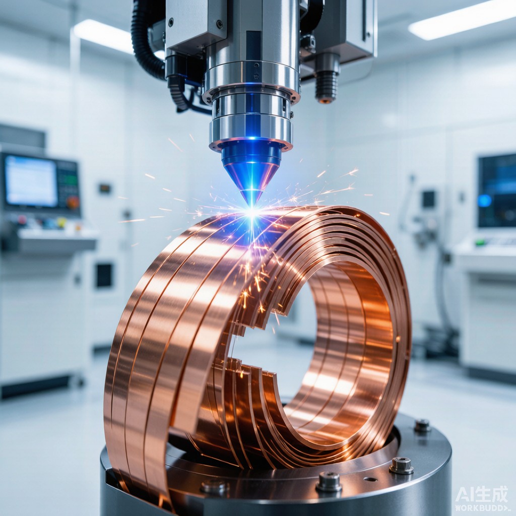
Precision SMT lead frames demand dimensional tolerances of ±0.01 mm on critical features including pin pitch, lead width, and dam-bar positions. As component packages shrink toward 0.3 mm pitch QFN and 01005 chip sizes, the manufacturing method for copper strip blanking directly impacts yield, tooling investment, and production flexibility. Two dominant technologies compete in this space: fiber laser cutting and progressive die mechanical blanking. This article provides a detailed engineering comparison of these processes for copper strip lead frame manufacturing, covering metallurgical effects, geometric precision, economic factors, and selection criteria.
Process Fundamentals
Fiber Laser Cutting of Copper Strip
Modern fiber lasers operating at 1,070 nm wavelength have overcome historical challenges with copper’s high reflectivity (≥95% at infrared wavelengths) through high brightness beam delivery and nitrogen assist gas. Key process parameters include:
- Laser power: 500W–2kW for 0.1–0.8 mm copper strip thickness
- Cutting speed: 2–8 m/min depending on thickness and edge quality requirements
- Assist gas: Nitrogen at 10–20 bar prevents oxidation and expels molten material
- Beam quality: M² < 1.2 enables spot sizes of 20–50 μm
- Focus position: Typically −0.1 to −0.3 mm below top surface for optimal edge quality
The laser cutting mechanism for copper involves localized melting and ejection by assist gas pressure. Unlike steel, copper’s high thermal conductivity (401 W/m·K) rapidly dissipates heat, requiring higher power density to maintain a stable cut front.
Progressive Die Mechanical Blanking
Progressive die stamping uses hardened tool steel punches and dies in a multi-station press to sequentially form, pierce, blank, and bend copper strip fed from coils. Critical parameters include:
- Punch-die clearance: 5–8% of strip thickness per side (e.g., 0.015–0.024 mm for 0.3 mm copper)
- Press speed: 200–800 strokes per minute for small lead frames
- Tool steel: D2, M2, or carbide for high-volume production
- Stripper force: 10–20% of blanking force to prevent punch adhesion
Edge Quality and Metallurgical Comparison
Edge Characteristics
| Parameter | Fiber Laser Cutting | Progressive Die Blanking |
|---|---|---|
| Edge roughness (Ra) | 3–8 μm | 0.5–2 μm (properly sharpened tools) |
| Heat-affected zone (HAZ) | 10–50 μm | None (cold deformation) |
| Burr height | 5–20 μm | 2–10 μm (with optimal clearance) |
| Edge taper | 0.5–2.0° | <0.1° |
| Recast layer | 2–10 μm oxidized copper | None |
| Microhardness at edge | +15–30% (rapid solidification) | +20–40% (work hardening) |
| Dross adhesion | Possible without optimized gas flow | None |
Thermal Effects on Microstructure
Laser cutting introduces a thin recast layer of resolidified copper with fine equiaxed grains (1–5 μm) and possible surface oxidation (Cu₂O, CuO) if oxygen ingress occurs. For SMT lead frames requiring subsequent plating, this oxide layer must be removed by acid pickle or mechanical brushing, adding a process step.
Mechanical blanking produces a characteristic edge profile with four zones: rollover (radius), burnish (sheared surface), fracture, and burr. The burnish zone exhibits severe plastic deformation with elongated grains aligned parallel to the shear direction. For copper alloys in H02 or H04 temper, the work-hardened edge zone (typically 20–50 μm deep) increases local hardness by 20–40%, which can affect subsequent lead forming and solderability if not properly managed.
Dimensional Accuracy and Geometric Capability
Precision Comparison
| Feature | Laser Cutting | Mechanical Blanking |
|---|---|---|
| Position accuracy | ±0.02–0.05 mm | ±0.005–0.01 mm |
| Minimum feature size | 0.05–0.10 mm (kerf limited) | 0.03–0.05 mm (tool strength limited) |
| Hole aspect ratio | Up to 5:1 (thickness:diameter) | Up to 3:1 |
| Internal corner radius | ≈0.5× kerf width (20–25 μm) | 0.05–0.10 mm (tool radius) |
| Taper compensation | Limited (0.5–2° inherent) | Excellent (<0.1°) |
| Repeatability (Cpk) | 1.0–1.33 | 1.33–1.67 |
For ultra-fine-pitch lead frames (0.3–0.4 mm pitch) with lead widths of 0.10–0.15 mm, progressive die blanking maintains superior positional accuracy and perpendicularity. Laser cutting’s inherent taper becomes problematic when lead thickness exceeds 0.5 mm or when strict coplanarity requirements (≤0.05 mm) apply.
Tooling and Economic Analysis
Cost Structure Comparison
| Cost Element | Laser Cutting | Mechanical Blanking |
|---|---|---|
| Initial tooling | $0 (programming only) | $15,000–$80,000 (progressive die) |
| Setup time | 15–30 minutes (program load) | 2–8 hours (die installation) |
| Tool life (punches/dies) | N/A | 2–10 million strokes (steel), 10–50M (carbide) |
| Per-part cycle time | 0.5–2.0 seconds | 0.075–0.3 seconds |
| Maintenance (per year) | $2,000–$5,000 (optics, nozzles) | $5,000–$20,000 (sharpening, replacement) |
| Material utilization | 85–92% (nesting dependent) | 75–85% (carrier strip required) |
| Design change cost | $0 (reprogram) | $2,000–$15,000 (die modification) |
Break-Even Analysis
For a typical SMT lead frame with a
ual volume of 500,000 pieces, progressive die blanking achieves lower per-part cost despite higher tooling investment. However, the break-even volume depends strongly on part complexity:
- Simple parts (low complexity): Break-even at 50,000–100,000 pieces/year
- Medium complexity: Break-even at 200,000–400,000 pieces/year
- High complexity (fine features, multiple bends): Break-even at 500,000+ pieces/year
Material-Specific Considerations
Copper Alloy Behavior
| Alloy | Laser Cut Quality | Blanking Performance | Key Consideration |
|---|---|---|---|
| C11000 (ETP Cu) | Excellent (low reflectivity with 1kW+) | Excellent | Standard reference |
| C19400 (CuFe2P) | Good (Fe increases absorption) | Excellent (higher strength) | Most common lead frame alloy |
| C19210 (CuFeP) | Good | Good | Lower Fe, softer than C19400 |
| C52100 (Phosphor Bronze) | Fair (Sn increases reflectivity) | Good | Higher tool wear in blanking |
| C7521 (CuNi18Zn20) | Fair (Ni/Zn affect absorption) | Fair (gummy chips) | EMI shielding applications |
Hybrid Manufacturing Strategies
Many Southeast Asian manufacturers employ hybrid approaches leveraging both technologies:
- Laser pre-blanking + die forming: Laser cuts complex outer profiles while progressive die handles precise piercing and lead forming in subsequent stations.
- Prototype-to-production transition: Laser cutting for prototype volumes (<10,000 pieces) and market validation, followed by progressive die investment after design freeze.
- Quick-change die inserts: Modular progressive dies with laser-cut insert blanks enable rapid design iteration without full die rebuilds.
Selection Decision Matrix
| Application Factor | Choose Laser Cutting | Choose Mechanical Blanking |
|---|---|---|
| A
ual volume |
<200,000 pieces | >300,000 pieces |
| Part complexity | High, frequent design changes | Stable, mature design |
| Lead pitch | >0.5 mm | <0.5 mm |
| Thickness range | 0.05–1.0 mm | 0.1–0.8 mm (optimal) |
| Edge quality priority | Acceptable with post-processing | Critical (plating, solderability) |
| Time-to-market | Days (no tooling) | Weeks (die design/build) |
| Capital investment limit | Low ($100K–$300K machine) | High ($500K+ with dies) |
Conclusion
For high-volume SMT lead frame production in Southeast Asian manufacturing environments, progressive die mechanical blanking remains the cost leader when a
ual volumes exceed 300,000 pieces and designs are stable. Its superior dimensional accuracy, perpendicular edges, and mature process control (Cpk ≥ 1.33) make it indispensable for fine-pitch packages.
However, fiber laser cutting has carved out essential roles in prototype manufacturing, low-to-medium volume production, and applications requiring rapid design iteration. Its zero tooling cost and 15-minute setup time enable just-in-time manufacturing strategies that progressive dies ca
ot match.
The optimal manufacturing strategy for most SMT component suppliers is a dual-capability approach: laser cutting for NPI and volume flexibility, progressive dies for high-volume mature products. This hybrid model maximizes capital efficiency while maintaining the quality and throughput required by modern electronics manufacturing.



