Introduction
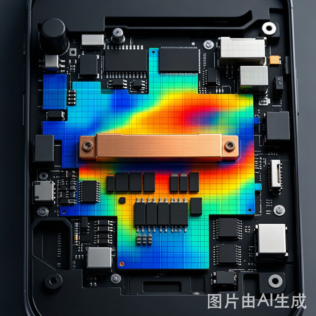
Modern consumer electronics pack ever-increasing power into ever-shrinking spaces. Smartphones, wearables, and compact IoT devices generate heat from processors, power management ICs, RF modules, and display drivers. When conventional heatsinks are too bulky, copper strip heat spreaders offer a thin, high-conductivity solution that distributes heat across the device enclosure or PCB before it reaches the ambient environment. Thermal simulation is the key to designing these heat spreaders correctly, ensuring that hot spots stay within acceptable limits without adding u
ecessary material or cost.
Why Copper Strip Heat Spreaders Are Effective
A heat spreader is not a heatsink. Instead of rejecting heat directly to the environment, a spreader redistributes heat from a small, intense heat source to a larger area. This larger area then couples to the enclosure, display, battery, or a dedicated heatsink. The effectiveness of a spreader depends on its in-plane thermal conductivity and the thermal resistance of the interfaces it crosses.
Copper strip is ideal for this role because it combines the highest thermal conductivity of any common engineering metal with the ability to be stamped into thin, complex shapes. A 0.1 mm to 0.3 mm thick copper strip can be integrated into the mid-frame of a smartphone or laminated into a flexible PCB, providing heat spreading with minimal thickness penalty.
Thermal Spreading Resistance Fundamentals
When heat flows from a small source into a large spreader, it encounters spreading resistance. This resistance is determined by the ratio of heat source area to spreader area, the thickness of the spreader, and the thermal conductivity of the material. For a circular heat source on an infinite thin plate, the spreading resistance can be approximated by analytical solutions, but real devices require finite element analysis (FEA) because the geometry is rarely simple.
Key parameters in spreading resistance include the spreader thickness, the location of the heat source, and the boundary conditions at the spreader edges. A thicker spreader reduces spreading resistance but increases weight and cost. Moving the heat source toward the center of the spreader generally improves performance by giving heat the shortest path to all edges.
Setting Up a Thermal Simulation Model
Geometry and Material Properties
The FEA model should include the copper strip spreader, the heat source, the thermal interface materials, and the surrounding structure. Material properties must be assigned carefully: copper conductivity at 400 W/m·K, stainless steel mid-frame at 15 W/m·K, aluminum at 160 W/m·K, and typical thermal interface materials at 1-10 W/m·K. Temperature-dependent conductivity should be used when the device operates across a wide temperature range.
Heat Source and Boundary Conditions
The heat source is typically modeled as a volumetric heat generation or a surface heat flux applied to the package footprint. The boundary conditions define how heat leaves the system. Common boundary conditions include convective cooling to air, radiation to surroundings, and conductive coupling to the device enclosure or battery. Ambient temperature and heat transfer coefficients should reflect the worst-case use scenario, such as a handheld device in a warm pocket or a wearable during exercise.
Meshing and Solver Considerations
Accurate thermal simulation requires adequate mesh resolution around the heat source and the spreader interfaces. The mesh should be refined in regions with high temperature gradients, such as the contact between the hot component and the copper strip. Steady-state analysis is usually sufficient for continuous operation, but transient analysis is needed for devices with pulsed workloads or rapid thermal changes.
Design Optimization Strategies
Thermal simulation enables rapid iteration of spreader design. Key optimization strategies include:
- Thickness tapering: Use thicker copper near the heat source where spreading resistance dominates, and thi
er material toward the edges where the heat flux is lower.
- Extended fingers: Add narrow copper extensions that reach toward the device enclosure or display, creating additional heat removal paths.
- Via stitching: For PCB-embedded spreaders, co
ect copper planes with thermal vias to improve vertical heat transfer.
- Interface optimization: Reduce thermal contact resistance by using thin, high-conductivity thermal gap fillers or phase-change materials between the spreader and the enclosure.
Validation and Testing
Simulation results must be validated against physical measurements. Infrared thermography and embedded thermocouples can map surface temperatures under controlled power conditions. Discrepancies between simulation and measurement often indicate inaccurate contact resistance assumptions or missing heat transfer paths. Calibration against a prototype ensures that the simulation can reliably predict performance across design variants.
Conclusion
Copper strip heat spreaders are a powerful tool for thermal management in compact SMT devices, but their performance depends heavily on geometry and integration. Thermal simulation provides the insight needed to optimize spreader thickness, shape, and placement before committing to tooling. By reducing thermal spreading resistance and eliminating hot spots, well-designed copper strip heat spreaders help smartphones, wearables, and IoT devices operate reliably within their thermal envelopes while maintaining the slim profiles consumers expect.



