In surface-mount technology (SMT) co
ector systems, the first few millimeters of mating motion determine whether a contact pair will deliver stable resistance over thousands of cycles. That motion is called contact wipe—the intentional sliding displacement between male and female terminals that scrapes through oxide films and establishes a clean metal-to-metal interface. Copper strip embossing and coining are two precision forming techniques used to engineer the wipe geometry, contact normal force, and localized hardness that govern long-term reliability. This article explains the process fundamentals, material choices, die design rules, and validation methods that separate high-performance SMT contacts from prematurely worn or oxidized interfaces.
Why Contact Wipe Matters for SMT Co
ectors
Contact resistance in a dematable co
ector is dominated by three interfacial phenomena: surface oxide layers, contaminant films, and the real area of metal contact under load. Without adequate wipe, the asperities that carry current can be isolated by a thin Cu2O or organic film, producing resistance fluctuations and localized heating. A well-designed wipe does three things simultaneously:
- Mechanical scrubbing: The sliding action breaks oxide scales and displaces debris.
- Fresh metal exposure: Clean copper or plated surfaces are pressed together under elastic or plastic deformation.
- Stable normal force: The residual spring force after mating must exceed the minimum needed to maintain conductivity across vibration and thermal cycling.
For SMT co
ectors used in automotive, industrial, and telecom equipment, typical wipe distances range from 0.3 mm to 1.5 mm, and normal forces fall between 0.5 N and 2.0 N per contact. The geometry that creates this behavior is often produced directly from copper strip using embossing or coining operations placed at strategic stations in a progressive die.
Embossing vs Coining: Process Fundamentals
Both embossing and coining are cold-forming operations performed on strip material, but they differ in how the metal is displaced and what dimensional outcome is achieved.
Embossing
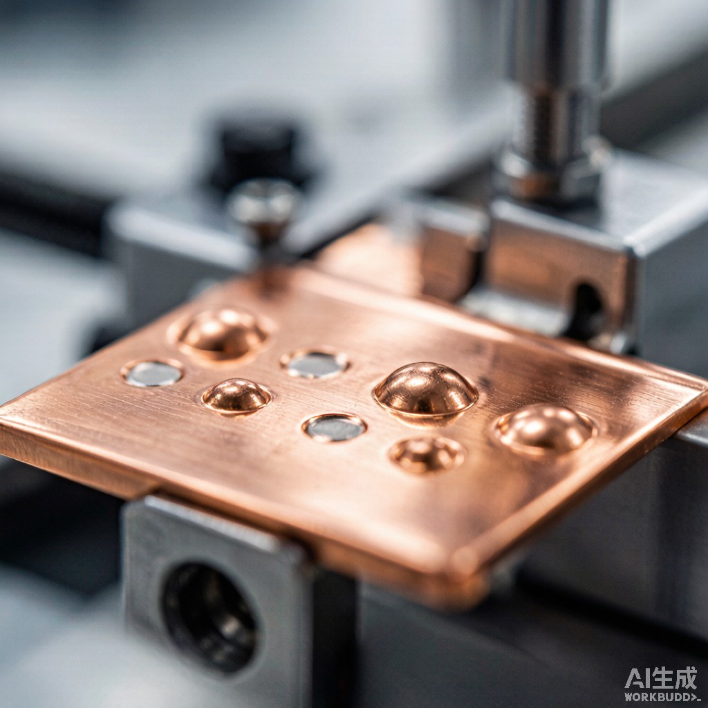
Embossing raises a localized feature above or below the original strip plane without significant thi
ing. A male punch and female cavity squeeze the copper, causing controlled plastic flow that creates a dome, rib, dimple, or cha
el. Because the feature is formed from the parent material, there is no loss of cross-section and the work-hardened region gains hardness and spring characteristics. Embossing is ideal for creating:
- Contact dimples that concentrate normal force into a small contact patch.
- Spring beams that provide compliant deflection during mating.
- Alignment ribs that guide terminals into position.
Typical emboss heights for SMT contacts range from 0.05 mm to 0.30 mm, depending on strip thickness and alloy ductility.
Coining
Coining compresses a defined volume of material between closed dies to produce precise thickness, surface finish, and edge definition. Unlike embossing, coining can reduce local thickness by 10–40% and generates very high compressive stresses that smooth surface asperities. Coining is used to:
- Create flat, mirror-like contact pads with controlled roughness (Ra 0.1–0.4 μm).
- Compress burr-free edges at wipe initiation points.
- Locally harden the contact zone to resist adhesive wear and fretting.
The choice between embossing and coining often depends on whether the design needs compliant spring action (embossing) or a hard, flat mating surface (coining). Many high-reliability contacts combine both: an embossed spring beam terminates in a coined contact pad.
Material Selection for Embossed and Coined Copper Contacts
Not all copper alloys respond identically to localized cold forming. The strip alloy must provide enough formability for embossing without cracking, yet enough strength and stress relaxation resistance to maintain force after years of service.
| Alloy | UNS | Temper | Yield Strength (MPa) | Conductivity (%IACS) | Best Use Case |
|---|---|---|---|---|---|
| ETP Copper | C11000 | H04 | 250–310 | 95–100 | Low-force signal contacts |
| Copper-Iron | C19400 | H08 | 450–520 | 60–65 | High-force power contacts |
| Phosphor Bronze | C51900 | H06 | 510–620 | 15–20 | Spring beams, high cycles |
| Beryllium Copper | C17200 | TH04 | 1,035–1,240 | 18–22 | Miniature high-reliability contacts |
| Nickel Silver | C75200 | H08 | 540–620 | 5–6 | Corrosion-resistant wear pads |
For cost-sensitive SMT co
ectors, C19400 in H08 temper is the workhorse: it offers excellent strength-to-conductivity balance and forms well in progressive dies. When extremely tight pitch or very high cycle life is required, C17200 beryllium copper delivers superior spring properties after age hardening.
Progressive Die Design Considerations
Embedding emboss and coin stations into a progressive die requires careful sequencing. The strip must remain flat enough to index through the press, yet locally deformed enough to create the desired contact geometry.
Station Sequence
A typical sequence for a coined contact pad might be: piercing → blanking → pre-form emboss → coining → final form → cut-off. Coining should generally occur before final bending to avoid distorting the carefully controlled contact surface. When both sides of the strip require features, simultaneous embossing reduces camber and twist.
Clearance and Punch Penetration
Coining dies run with near-zero clearance (1–3% of strip thickness) compared with conventional blanking clearances of 5–10%. Punch penetration must be sufficient to generate hydrostatic compression but not so deep that the strip thins excessively or tears. Pilot pins and stock guides must account for local thickness variation after coining.
Lubrication and Tool Steel
Copper alloys tend to gall against unlubricated tool steel. A chlorine-free stamping oil with EP additives reduces galling and extends tool life. For high-volume production, punch and die materials such as M2 high-speed steel, D2 tool steel, or tungsten carbide inserts are preferred. TiCN or AlCrN PVD coatings further reduce adhesive wear and allow higher stamping speeds.
Quality Validation and Testing
After forming, contacts must be validated for geometry, mechanical performance, and electrical reliability.
- Dimensional inspection: Optical comparators or 3D optical profilometers verify emboss height, coin thickness, radius, and wipe angle.
- Microhardness: Vickers or Knoop hardness testing across the coined zone confirms work-hardening consistency.
- Contact resistance: Four-wire measurements at rated current after specified mating cycles detect oxidation or wear degradation.
- Wear testing: Automated insertion/extraction testers run 500–10,000 cycles while monitoring normal force decay.
- Thermal aging: Samples aged at 105°C or 125°C evaluate stress relaxation and force retention.
Application Guidelines
When specifying embossed or coined SMT copper contacts, designers should balance electrical, mechanical, and manufacturability requirements:
- Define the required wipe distance and normal force before selecting alloy and temper.
- Place coined pads on the side of the terminal that interfaces with the mating contact; avoid secondary operations that could scratch the surface.
- Keep emboss-to-edge distances at least 1.5× material thickness to prevent splitting.
- Specify surface finish and plating (tin, nickel-gold, or silver) after forming to protect the active contact zone.
- Validate under worst-case thermal and vibration conditions relevant to the end application.
Conclusion
Copper strip embossing and coining transform flat strip material into functional contact interfaces with engineered wipe, force, and hardness. By selecting the right alloy, sequencing die operations correctly, and validating parts through mechanical and electrical testing, manufacturers can produce SMT co
ectors that maintain stable performance across demanding operating lifetimes.



