Introduction
Solder joints are the mechanical and electrical lifelines of SMT assemblies, but they are also the most common failure point under thermal and mechanical stress. Lead-free SAC (Sn-Ag-Cu) solders exhibit fundamentally different creep and fatigue behavior than legacy Sn-Pb solders, and understanding these mechanisms is essential for designing reliable electronics for automotive, aerospace, and industrial applications. This article explores the metallurgical mechanisms of solder joint failure and the qualification methods that predict field life.
Why Lead-Free Solders Behave Differently
Traditional Sn63/Pb37 solder has a melting point of 183°C and operates at homologous temperatures (operating temperature divided by melting point in Kelvin) of 0.6-0.7 in typical electronics applications. SAC305 (Sn96.5/Ag3.0/Cu0.5) melts at 217°C, so the same 100°C operating temperature produces a homologous temperature of approximately 0.65 — still in the creep-sensitive regime.
The microstructural difference is significant. Sn-Pb solder has a two-phase microstructure (tin-rich beta phase and lead-rich alpha phase) that provides natural grain boundary strengthening. SAC solders are nearly pure tin with dispersed Ag₃Sn and Cu₆Sn₅ intermetallic particles. Under cyclic stress, the tin grains recrystallize and coarsen, and the intermetallic particles redistribute, leading to accelerated creep and fatigue damage compared to Sn-Pb.
Creep Mechanisms in SAC Solders
Creep is the time-dependent plastic deformation of a material under constant stress at elevated temperature. For SAC solders in typical SMT operating conditions (25-125°C), the dominant creep mechanisms are:
Dislocation Glide-Climb
The dominant mechanism at high stresses and lower temperatures. Dislocations move along slip planes and “climb” around obstacles via vacancy diffusion. In SAC solders, the dispersed Ag₃Sn and Cu₆Sn₅ particles pin dislocations, providing some strengthening — but the obstacles coarsen over time at elevated temperature, reducing their effectiveness.
Grain Boundary Sliding
Dominant at lower stresses and higher temperatures. Adjacent tin grains slide past each other along their boundaries, accommodated by diffusion along the boundary. The tin-tin grain boundaries in SAC solders are particularly susceptible because they lack the second-phase strengthening present in Sn-Pb.
Diffusional Creep (Nabarro-Herring / Coble)
At very low stresses and high homologous temperatures, vacancy diffusion through the bulk or along grain boundaries produces strain. This mechanism is typically secondary in SMT solder joints, but it contributes to the long-term deformation observed in high-temperature automotive under-hood applications (above 150°C).
Intermetallic Compound (IMC) Growth
At the interface between solder and copper pad, a layer of Cu₆Sn₅ intermetallic forms during reflow. This layer is essential for a metallurgical bond, but its growth continues throughout the assembly’s service life, driven by diffusion of copper atoms into the tin matrix. As the IMC layer thickens, several detrimental effects emerge:
- The IMC layer is brittle compared to the surrounding solder, creating a potential crack initiation site
- Cu₆Sn₅ can transform to Cu₃Sn at the copper interface, which is even more brittle and prone to Kirkendall void formation
- Excessive IMC growth consumes the copper pad, weakening the pad-to-trace co
ection
- The IMC layer has different CTE than both solder and copper, increasing thermal stress at the interface
For SAC305 on copper, IMC layer thickness after reflow is typically 1-3 µm. After 1000 hours of aging at 150°C, the layer can grow to 8-12 µm. SAC solder alloys with higher silver content (SAC405, SAC405 plus bismuth or nickel dopants) form slightly thicker initial IMC layers but exhibit better high-temperature reliability due to refined microstructure.
Thermal Cycling and Thermal Fatigue
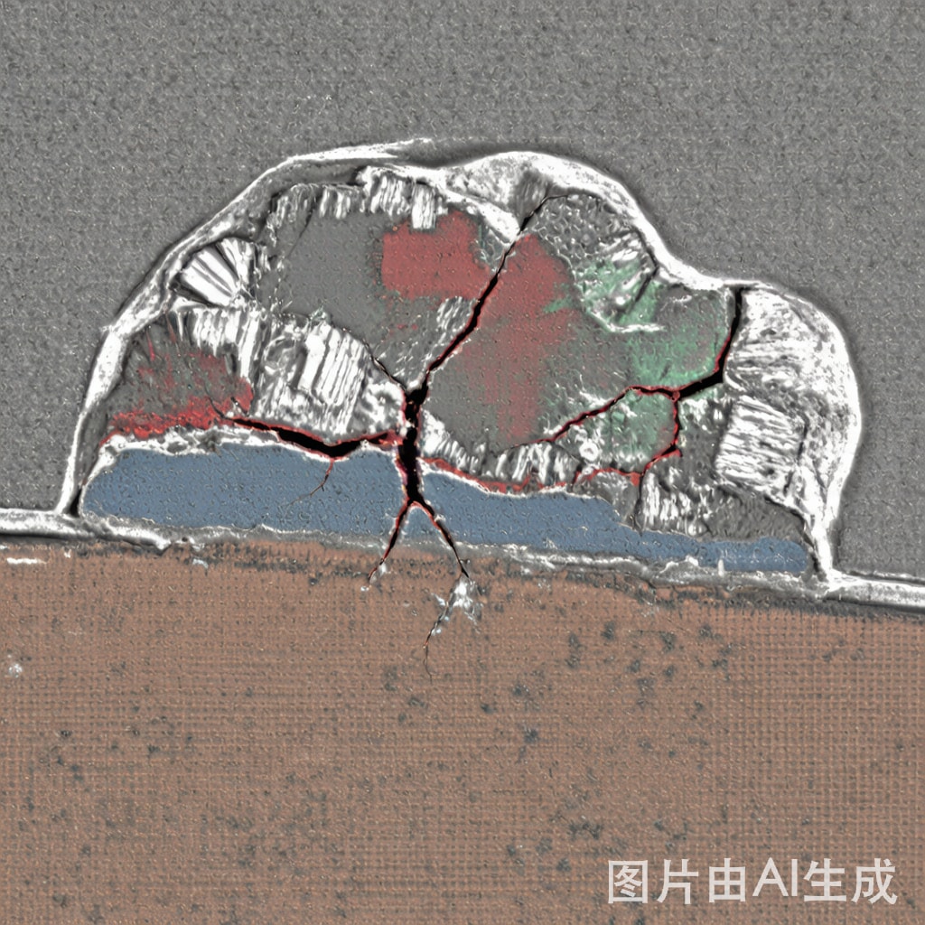
The CTE mismatch between component (3-7 ppm/°C for silicon, 6-8 ppm/°C for ceramic) and PCB (14-17 ppm/°C for FR-4) creates cyclic shear stress on solder joints during temperature changes. Each thermal cycle produces microplastic strain that accumulates over time, eventually leading to crack initiation, propagation, and electrical failure.
The characteristic failure mode in thermal cycling is crack propagation through the solder joint, typically near the component-side intermetallic interface or within the bulk solder near the high-stress region. Cross-sectioning of failed parts typically shows a fatigue crack extending across 50-90% of the joint cross-section, with the remaining ligament providing intermittent contact that eventually opens completely.
IPC-9701 Thermal Cycling Qualification
IPC-9701 (“Performance Test Methods and Qualification Requirements for Surface-Mount Solder Attachments”) defines the standard thermal cycling protocols for solder joint reliability qualification. The two most common test profiles are:
- TC1 (0/100°C): 0°C to 100°C, 10-15 minute dwell, 10-15 minute ramp — typical for consumer and commercial electronics
- TC3 (-40/+125°C): -40°C to 125°C, 15-30 minute dwell, slower ramps — typical for automotive and industrial applications
- TC4 (-55/+125°C): Military/aerospace grade temperature extremes
Failure is typically defined as a 20% increase in electrical resistance or complete open circuit. SAC305 solder joints in BGAs typically achieve 1,500-3,000 cycles to failure in TC1 conditions and 500-1,500 cycles in TC3 conditions. Components with larger CTE mismatch, higher standoff heights, and aggressive thermal cycling see shorter life.
Finite Element Modeling (FEA) of Solder Joints
Modern solder joint reliability prediction relies heavily on FEA, which models the visco-plastic stress-strain behavior of SAC solders under cyclic loading. A typical FEA workflow includes:
- Build a 2D or 3D model of the solder joint geometry, including the BGA pad, via, and PCB trace
- Assign material properties: elastic modulus, Poisson ratio, CTE, and creep parameters (typically the Garofalo-Arrhenius model for SAC alloys)
- Apply thermal cycling boundary conditions matching the qualification profile
- Calculate accumulated creep strain per cycle using the Modified Coffin-Manson relationship
- Predict cycles to failure based on the accumulated strain criterion
FEA can predict relative reliability differences between design alternatives (e.g., solder mask defined vs non-solder mask defined pads, different ball alloys, different via-in-pad configurations) without the cost of physical prototyping. However, model accuracy depends on the quality of the constitutive model parameters for the specific solder alloy — generic SAC305 properties can introduce 20-40% error in cycle-to-failure prediction.
Design Strategies for Improved Reliability
Several design and material strategies can extend solder joint life under thermal cycling:
- Component standoff height: Taller solder joints (e.g., sphere-on-pad vs collapsed-joint configurations) distribute strain over a larger volume, extending life
- Underfill: For BGAs on high-CTE substrates, capillary underfill redistributes thermal stress from individual solder joints to the entire package, typically extending life by 5-10×
- Alloy selection: SAC405 (4% Ag) or SAC-Q (with bismuth) provides better thermal fatigue resistance than SAC305 for high-temperature applications
- PCB material: High-Tg, low-CTE PCB laminates (e.g., FR-4 with Tg 170°C and CTE 12-14 ppm/°C) reduce the CTE mismatch with components
- Thermal management: Reducing peak operating temperature by 10°C can extend solder joint life by 2-3× in many cases
Conclusion
Solder joint reliability in lead-free SMT assemblies is governed by a complex interplay of creep, fatigue, and intermetallic growth mechanisms that differ fundamentally from legacy Sn-Pb behavior. SAC solders are more sensitive to thermal cycling and high-temperature aging, but careful design choices — including alloy selection, standoff height, underfill application, and PCB material — can extend service life to meet automotive and aerospace qualification requirements. FEA modeling combined with IPC-9701 thermal cycling testing provides a robust methodology for predicting and validating solder joint reliability before committing to high-volume production, reducing field failure risk and supporting long-term product reliability commitments.