Introduction
Modern electronics increasingly combine multiple interco
ection technologies on a single PCB: SMT soldering for passive and active components, wire bonding for bare die or COB (chip-on-board), and press-fit co
ectors for high-current or high-reliability interfaces. Each of these interco
ection methods imposes different requirements on the PCB surface finish, and ENEPIG — Electroless Nickel, Electroless Palladium, Immersion Gold — has emerged as the universal solution that satisfies all three simultaneously.
What Is ENEPIG?
ENEPIG is a tri-layer surface finish deposited on copper pads through a series of autocatalytic and immersion chemical processes:
- Electroless Nickel (3-6 µm): The diffusion barrier layer that prevents copper from migrating into the solder joint or gold wire bond interface. Nickel also provides the hard, flat surface needed for wire bonding and press-fit applications.
- Electroless Palladium (0.05-0.15 µm): The critical middle layer that distinguishes ENEPIG from ENIG. Palladium serves as a protective layer that prevents nickel oxidation and eliminates the “black pad” defect associated with ENIG. It also acts as an oxidation barrier during thermal excursions.
- Immersion Gold (0.05-0.12 µm): The top layer providing oxidation resistance, excellent solderability, and reliable wire bonding surface. The thin gold layer dissolves completely into the solder joint during reflow, leaving a clean palladium surface for solder wetting.
Comparison with ENIG
ENIG (Electroless Nickel Immersion Gold) has been the industry-standard surface finish for decades, but it suffers from a well-documented reliability risk: black pad syndrome. This occurs when excessive galvanic corrosion of the nickel layer during the immersion gold deposition process creates a phosphorus-rich, brittle nickel surface that fails under mechanical stress.
ENEPIG eliminates this failure mode because the electroless palladium layer is deposited before the immersion gold. The palladium protects the nickel from the corrosive gold bath, preventing hyper-corrosion. The result is a uniform, defect-free nickel-phosphorus layer with consistent mechanical properties.
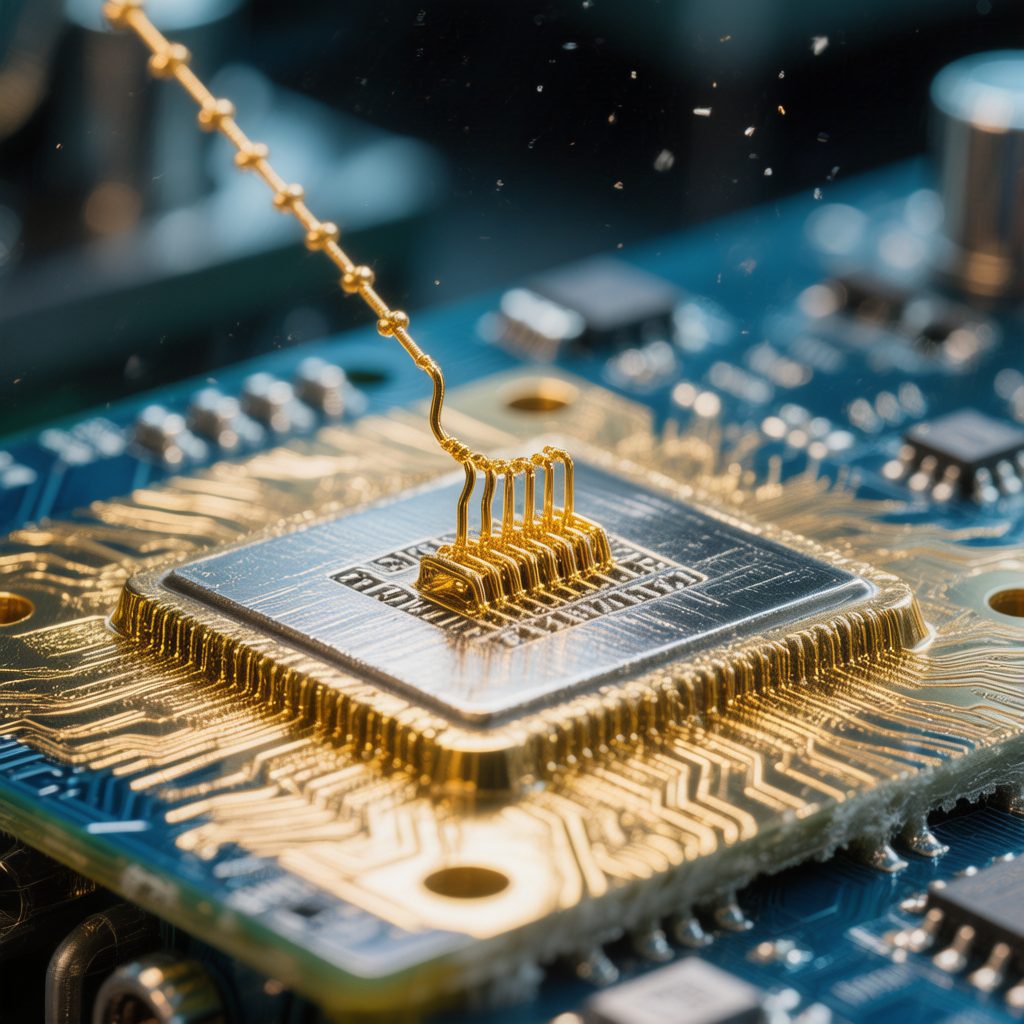
Wire Bonding Compatibility
For applications requiring wire bonding alongside SMT assembly, ENEPIG offers unique advantages. The palladium layer provides a hard, smooth surface ideal for both gold and copper wire bonding:
- Gold wire bonding: The thin immersion gold layer on ENEPIG provides an excellent surface for gold wire bonding with pull strengths comparable to electrolytic Ni/Au. The palladium underneath prevents nickel diffusion into the gold layer during thermal aging, maintaining bond reliability over time.
- Copper wire bonding: Copper wire bonding on ENEPIG has gained significant traction in semiconductor packaging. The palladium layer protects against oxidation during the bonding process, and copper wire on palladium forms reliable intermetallic bonds with excellent electrical performance.
Solder Joint Reliability
During SMT reflow, the thin immersion gold layer dissolves rapidly into the molten solder, exposing the palladium surface. SAC305 solder wets the palladium surface effectively, forming a reliable solder joint with the nickel barrier layer. The absence of a thick gold layer (unlike ENIG with its variable gold thickness) prevents gold embrittlement — a condition where excessive gold in the solder joint forms brittle AuSn₄ intermetallics.
Thermal cycling tests per IPC-9701 show ENEPIG solder joints achieving 2,500-4,000 cycles to failure, comparable to or exceeding ENIG performance, with the additional benefit of eliminating black pad as a failure mechanism.
Press-Fit Co
ector Compatibility
Press-fit technology relies on the interference fit between a compliant pin and a plated through-hole. The surface finish must provide consistent hole diameter, low insertion force, and reliable gas-tight electrical contact. ENEPIG’s combination of hard nickel and smooth palladium/gold surface meets all these requirements, making it the preferred finish for boards that combine SMT components with press-fit backplane co
ectors.
Cost and Application Guidance
ENEPIG carries approximately a 20-30% cost premium over ENIG due to the additional palladium plating step and the precious metal content. This premium is justified when the PCB requires two or more of the following: SMT soldering, wire bonding, press-fit co
ections, or extended shelf life (>12 months). For standard SMT-only assemblies, ENIG or immersion silver may provide adequate performance at lower cost.
Conclusion
ENEPIG has earned its reputation as the universal surface finish for mixed-technology PCB assembly. By combining the solderability of ENIG with the wire bonding capability of electrolytic Ni/Au and the press-fit compatibility of hard nickel, ENEPIG enables designers to specify a single surface finish for boards that integrate multiple interco
ection technologies. The elimination of black pad risk alone justifies the cost premium for high-reliability applications, while the extended shelf life and process flexibility add further value across the product lifecycle.