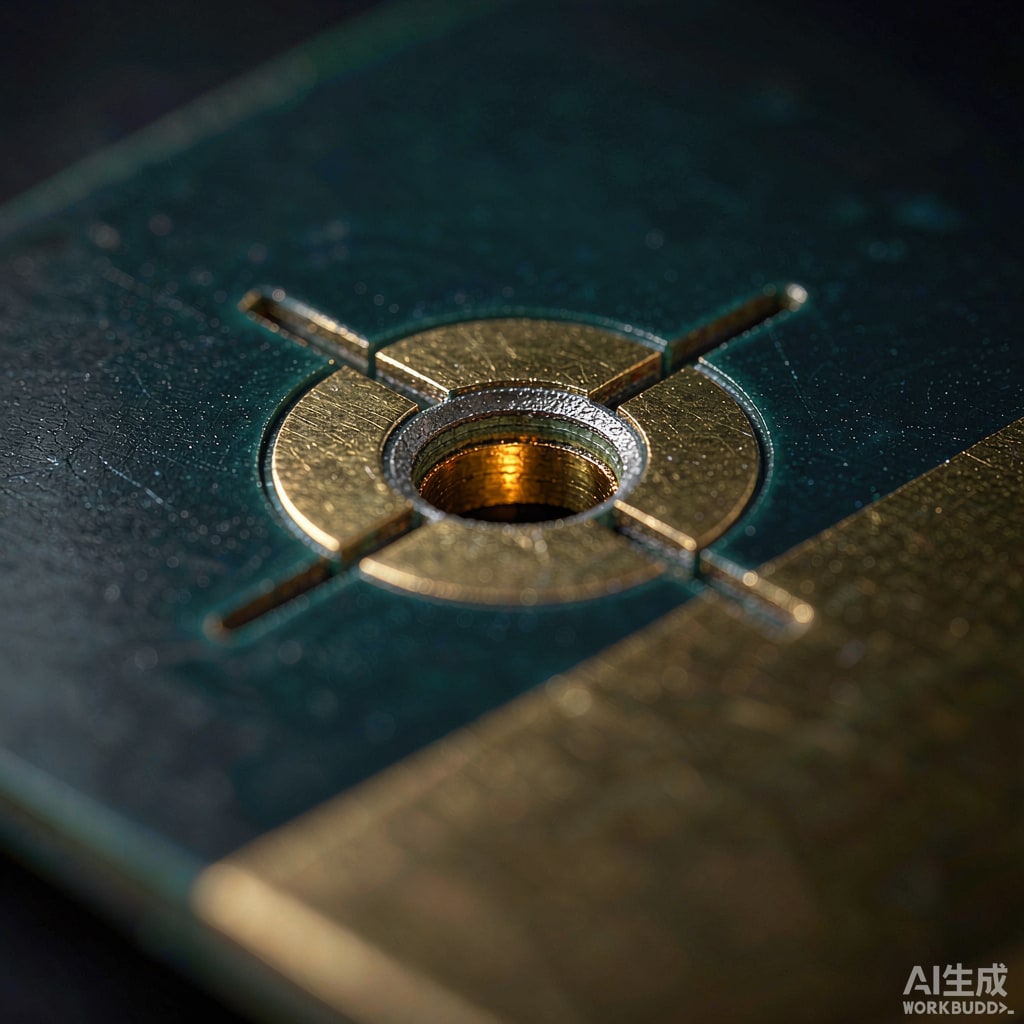
A thermal relief is one of the few PCB features that exists purely to make manufacturing easier, and it does so by making the electrical and thermal job harder. Four narrow spokes and a gap in the plane slow heat conduction out of a pad so a soldering iron or a wave can actually reach temperature. That same restriction sits in the middle of the conduction path for every watt the component needs to shed.
Most boards inherit their spoke geometry from a CAD library default. On a signal pad that is fine. On a power pad carrying two watts, or a co
ector pin tied to a ground plane that also serves as a heat spreader, the default can be the difference between a 15 K rise and a 45 K rise. This guide puts numbers on the trade-off.
What a Thermal Relief Actually Does
A relief replaces a solid pad-to-plane co
ection with three or four narrow spokes separated by etched gaps. The spoke is a short, narrow, thin conductor: length equal to the antipad a
ulus, width equal to the spoke width, thickness equal to the copper weight. Its thermal resistance follows the standard conduction relation, R equals length divided by the product of conductivity, cross sectional area and spoke count.
Take a realistic case. Four spokes, 0.40 mm wide, 35 micrometre copper, 0.50 mm long, copper conductivity 385 W per metre kelvin. The area of one spoke is 0.40 mm times 0.035 mm, or 1.4 times ten to the minus eight square metres. Its resistance is 0.50 mm divided by 385 times that area, about 93 K per watt. Four in parallel give roughly 23 K per watt. Push 2 W through that co
ection and the pad sits 46 K above the plane. Had the pad been solidly co
ected, the same 2 W would see a resistance closer to 2 K per watt.
That is the entire argument in one calculation. Relief buys solderability at a thermal cost of tens of kelvin per watt.
The Cost of Too Much Relief
Too little relief produces cold joints, incomplete hole fill, blowholes and, on wave solder, icicling and bridging at the drag direction. The mechanism is simple: the plane absorbs heat faster than the nozzle can supply it, the barrel walls never exceed solder liquidus for long enough, and capillary flow stalls. IPC-A-610 requires 75 percent vertical fill for Class 2 and 75 percent for Class 3 with additional criteria on the barrel; a relief that is too tight routinely lands at 40 to 60 percent.
The usual reaction is to shrink the spokes further until the joint looks acceptable. That fixes the visual and breaks the thermal path. A better approach is to decide which requirement is primary and engineer the other one around it.
Sizing Spokes Deliberately
Rule of thumb for through-hole
For a typical 1.0 mm finished hole with a 1.8 mm pad, four spokes of 0.30 to 0.40 mm with 0.25 to 0.30 mm gaps solder reliably on a properly profiled wave. For pads above 2.5 mm, or pins on a 3 mm grid with heavy planes, widen to 0.50 mm and accept a longer contact time. Total spoke width across any diameter should stay below about 50 percent of the pad perimeter; above that the relief stops relieving.
I
er layers matter as much
A relief on the top layer only does nothing if the same net co
ects solidly on layer 2. If the goal is solderability, place the relief on every plane layer the pin passes through, offsetting spoke angles by 45 degrees between layers so the antipad does not create a continuous thermal tu
el. If the goal is heat spreading, do the opposite and keep one plane layer solid while relieving the outer layers only.
Antipad and clearance
The gap width sets both thermal resistance and etch yield. Below 0.20 mm, etchant traps and undercut become a manufacturing risk. Between 0.25 and 0.35 mm is the practical sweet spot for 1 oz copper. Beyond 0.50 mm the joint solders easily but the spokes become the only thermal path and the number gets ugly fast.
SMT Pads Are a Different Problem
Reflow does not steal heat through the plane the way a wave does, but a large plane still changes the heating profile locally. A 0402 chip capacitor with one pad tied to a ground plane and the other tied to a thin trace heats asymmetrically, and the solder on the plane side lags by several seconds. That asymmetry is the classic recipe for tombstoning and for one-sided fillets. Two remedies work: a relief on the plane-co
ected pad, or a matched copper balance on the opposite pad so both sides heat at the same rate. The second is usually better because it costs no thermal performance.
For exposed pads on QFN and DFN packages, relief is the wrong tool entirely. The exposed pad needs maximum conduction, which means solid co
ection plus a via array. Blocking that path to improve reflow is counterproductive; instead fix the profile and the stencil.
Thermal via arrays under exposed pads
A 0.30 mm drill with 25 micrometre plating has a barrel resistance of roughly 60 to 100 K per watt, dominated by the plating cross section. Nine vias on a 1.0 mm pitch under a 5 mm exposed pad give an effective 7 to 11 K per watt, which is a far better investment than widening spokes. Fill and cap them if the pad is also a solderable surface, per IPC-4761 Type VII, and keep the via pitch tight enough that the copper between them does not become the bottleneck.
When Direct Co
ection Is the Right Answer
Three cases justify deleting the relief: high current paths where a few tens of milliohms matter, RF and high speed ground returns where spoke inductance raises the return path impedance, and EMC critical chassis ground pins. In each case the soldering problem has to be solved another way, and it usually can be: longer preheat, a smaller nozzle with higher mass flow, selective solder with a dedicated thermal profile, or a press-fit pin that needs no solder at all.
Verifying the Compromise
Two measurements settle most arguments. First, thermal: power the board at rated load, wait for steady state, and read the pad and plane temperatures with fine thermocouples or a thermal camera at 50 micrometre resolution. A 40 K delta across a spoke pair confirms the relief is throttling. Second, process: cross section one assembly per lot and measure barrel fill, then X-ray the exposed pad joints for void area. Voiding above 25 percent on a thermal pad means the conduction path is losing its interface, and no amount of spoke tuning will recover it.
The design rule that survives both tests is simple. Choose the relief to satisfy the soldering process with the smallest acceptable gap, then recover thermal performance with vias and plane area rather than with spokes. Spokes are a process feature. Vias are a thermal feature. Confusing the two is how boards end up both hard to solder and too hot.