The Failure Mode Nobody Names
Most PCB thermal discussions focus on a single hot component and its junction temperature. But on dense SMT assemblies — where passives, oscillators, sensors, and power devices share a few square centimeters — the dominant thermal problem is often thermal crosstalk: heat from one component raising the temperature of neighbors that were never designed to run hot. A 2°C drift on a voltage reference becomes a gain error in your analog front end. A crystal ru
ing 15°C above ambient shifts frequency beyond its calibration budget. An electrolytic capacitor ru
ing 10°C hot halves its life. None of these parts fail a junction-temperature check; they fail the system specification.
How Heat Actually Spreads on a Board
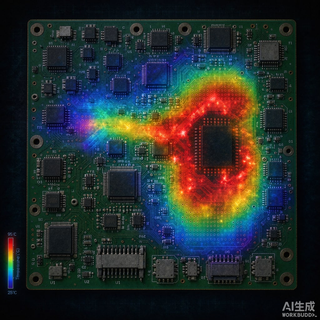
Thermal crosstalk travels through three paths. Conduction through copper is usually dominant: ground planes and power planes are excellent lateral heat spreaders, so a hot QFN deposits heat across the entire plane it sits on. Convection from surfaces warms the air inside the enclosure, raising ambient for everything. Radiation contributes 10–25% in still-air conditions, from hot component tops to anything with a line of sight.
The key insight for layout engineers: the copper plane that improves your hot component’s cooling is the same plane that delivers that heat to your sensitive components. Thermal vias under a power device, celebrated as good practice, pump heat into the ground plane — where your precision reference is probably sitting.
Identifying Crosstalk Risk Early
During schematic review, classify every component into three thermal sensitivity tiers. Tier 1 (drift-critical): voltage references, precision resistors, crystal and MEMS oscillators, temperature sensors, analog front ends. These care about absolute temperature and gradients. Tier 2 (life-limited): electrolytic and polymer capacitors, LEDs, optocouplers. These care about average operating temperature. Tier 3 (heat sources): power converters, LDOs, RF PAs, motor drivers, FPGAs. During placement review, require a minimum thermal separation from Tier 3 to Tier 1 components — a practical rule of thumb is 10–15 mm on a 4-layer board with continuous planes, more if the plane is interrupted.
If you have a thermal camera and a bench supply, a 30-minute experiment beats any spreadsheet: power only the heat sources and map the board surface. Locations where Tier 1 components exceed 5°C above board ambient are your problem spots.
Layout Tactics to Break the Heat Path
Plane Cutting and Thermal Moats
The most powerful tool is a deliberate slot or moat in the copper plane between a major heat source and the sensitive zone. A 1–2 mm slot across all copper layers forces heat to travel around, lengthening the conduction path and dropping the temperature at the far side by several degrees. The cost is real, though: a moat interrupts return currents. Treat it like a signal-integrity decision — route the affected return paths explicitly, and keep the moat away from high-speed differential pairs. On i
er layers, thermal relief spokes around plane-co
ected vias in the sensitive zone add small but useful thermal resistance.
Component-Level Isolation
Where a moat is impossible, use the stack-up. Putting the power section on the board bottom with the analog section directly above it on the top is a classic mistake — heat conducts straight through the 1.6 mm laminate (FR-4 is a poor insulator thermally at these distances). Instead, separate heat sources and sensitive components horizontally by at least one intermediate component position, and orient hot components so their dominant convection plume (upward, in natural convection) does not sweep over Tier 1 parts. In forced-air designs, place sensitive components upstream of heat sources relative to airflow, never downstream.
Copper Pours and Their Double Edge
Local copper pours around hot components help them, but a pour that touches the sensitive zone merely extends the crosstalk path. If you tie a local pour under an LDO to the ground plane with many vias, you are deliberately moving LDO heat into the plane — fine if the plane can dissipate it somewhere useful, harmful if the plane edges terminate next to your analog island. Decide where the heat goes, not just how to move it.
Enclosure and System-Level Measures
Board-level tactics reach their limit when the whole enclosure heats up. If internal air temperature climbs, every component inherits the penalty. Simple wins: conductive coupling from hot components to the metal enclosure (thermal pads to the lid), orientation of the enclosure for chimney effect in passive designs, and shielding cans only around the analog island — a can also acts as a radiation shield and a small heat spreader, which sometimes helps Tier 1 components even as it blocks airflow.
Verifying the Result
Close the loop with three measurements on the first article: IR imaging under realistic load, contact thermocouples on the two or three most drift-sensitive components, and a functional check of the parameters that crosstalk would corrupt (reference voltage versus temperature, oscillator frequency, ADC offset). If a parameter moves 2× more than your error budget predicts between cold start and thermal steady state, crosstalk is likely still leaking through a path you have not found — and the IR map usually shows where.
Thermal crosstalk is rarely fatal; it is quietly expensive. A placement review that explicitly names thermal sensitivity tiers, and a design rule of thermal separation between heat sources and precision analog, will eliminate the majority of these problems before the first spin.