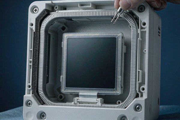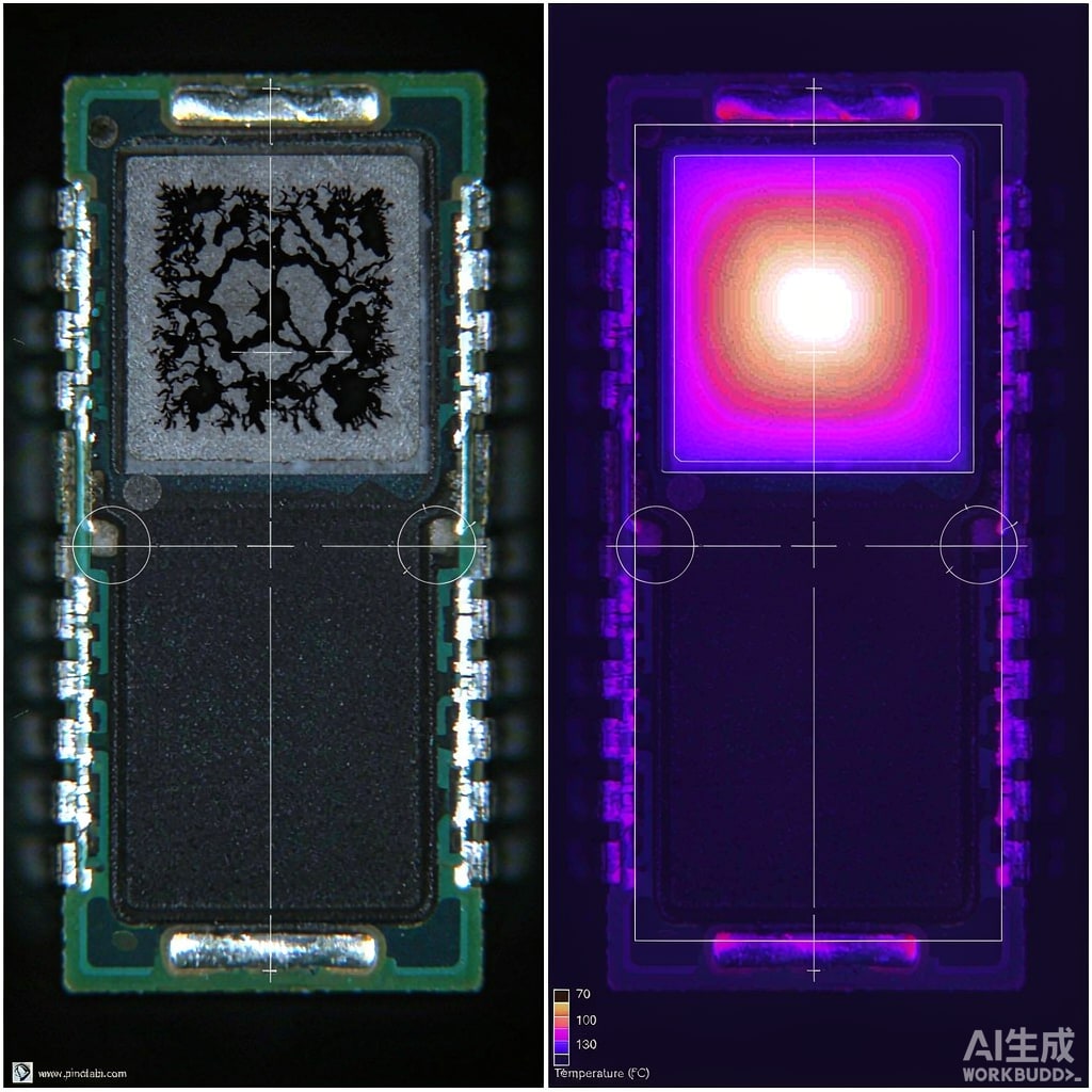
Power semiconductor packages such as DPAK, D2PAK, QFN, and LFPAK rely on a solder joint between the exposed thermal pad and the PCB land to conduct heat away from the die. That joint is also the most common location for solder voids—gas pockets trapped in the intermetallic layer. While a few small voids are normal, excessive voiding can raise thermal resistance, accelerate electromigration, and reduce long-term reliability. This article explains how voids affect heat transfer, how to measure them, and how to keep them within acceptable limits.
How Voids Increase Thermal Resistance
The thermal resistance of a solder joint is dominated by its thickness and effective thermal conductivity. Solder alloys have much lower conductivity than copper or aluminum, so even a thin solder layer adds resistance. When voids occupy part of the joint area, the heat must spread around the voids, effectively lengthening the conduction path and increasing the overall thermal resistance.
For a typical SAC305 solder joint, a void area of 25% can increase thermal resistance by 15–30%, depending on void distribution. A single large void under the center of the thermal pad is worse than many small voids spread across the pad because it blocks the direct path from the die hot spot to the PCB copper. In high-current applications, that temperature rise can push a MOSFET or LED driver out of its safe operating area.
Common Causes of Voids
Voids form when flux volatiles, moisture, or solder paste oxides ca
ot escape before the solder solidifies. The main process contributors are:
- Excessive solder paste volume traps flux vapor under the pad.
- Insufficient preheat does not allow solvents to evaporate before reflow.
- Low soak temperature limits flux activation and oxide reduction.
- Poor pad design without escape cha
els for outgassing.
- Oxidized surfaces on the package pad or PCB land reduce wetting.
Moisture absorbed by the component molding compound can also outgas during reflow, creating package-side voids known as popcorning. Proper dry-pack handling and floor life control are essential for large power packages.
Inspection Methods
X-ray inspection is the most common way to evaluate voids in production. Modern 2D X-ray systems can detect voids down to roughly 2–5% of pad area, while 3D X-ray laminography provides depth information and is better for stacked or complex joints. Acoustic microscopy (C-SAM) can detect delaminations and voids near interfaces but is slower and typically reserved for failure analysis.
Report voids as a percentage of the total thermal pad area, not just as a count. Industry guidelines such as IPC-A-610 and customer-specific standards often set limits between 10% and 50%, depending on application criticality. For high-reliability automotive or industrial power electronics, a common target is below 10% total void area with no single void larger than 5%.
Design and Process Mitigation
The most effective way to reduce voids is to give flux vapor a path to escape. This is usually done by dividing the thermal pad into an array of smaller pads with solder mask-defined cha
els, or by using a window-pane pattern in the solder paste stencil. Reducing paste coverage from 100% to 50–70% of the pad area often lowers voids without sacrificing thermal performance.
Other practical measures include:
- Using type 4 or type 5 solder paste with lower oxide content for fine-pitch power pads.
- Extending the preheat zone to 150–180°C and increasing soak time to volatilize flux carriers.
- Applying nitrogen reflow to improve wetting and reduce oxide formation.
- Specifying a minimum PCB land flatness and plating quality to avoid trapped gas pockets.
Thermal Validation
Even with low void area, the final test is thermal. Measure the case temperature or junction temperature under operating conditions using a thermocouple, infrared camera, or the device’s internal temperature sensor. Compare the measured value to a thermal model and look for unexpected hotspots. If the measured temperature is more than 10°C above simulation, investigate the solder joint quality as a first suspect.
Conclusion
Solder voids under SMT power pads are not automatically a defect, but they must be controlled. By designing escape paths, optimizing reflow profiles, and using quantitative inspection, manufacturers can keep voids within limits that preserve thermal performance and reliability. Specify void acceptance criteria up front and verify them with X-ray to avoid late-stage thermal failures in the field.