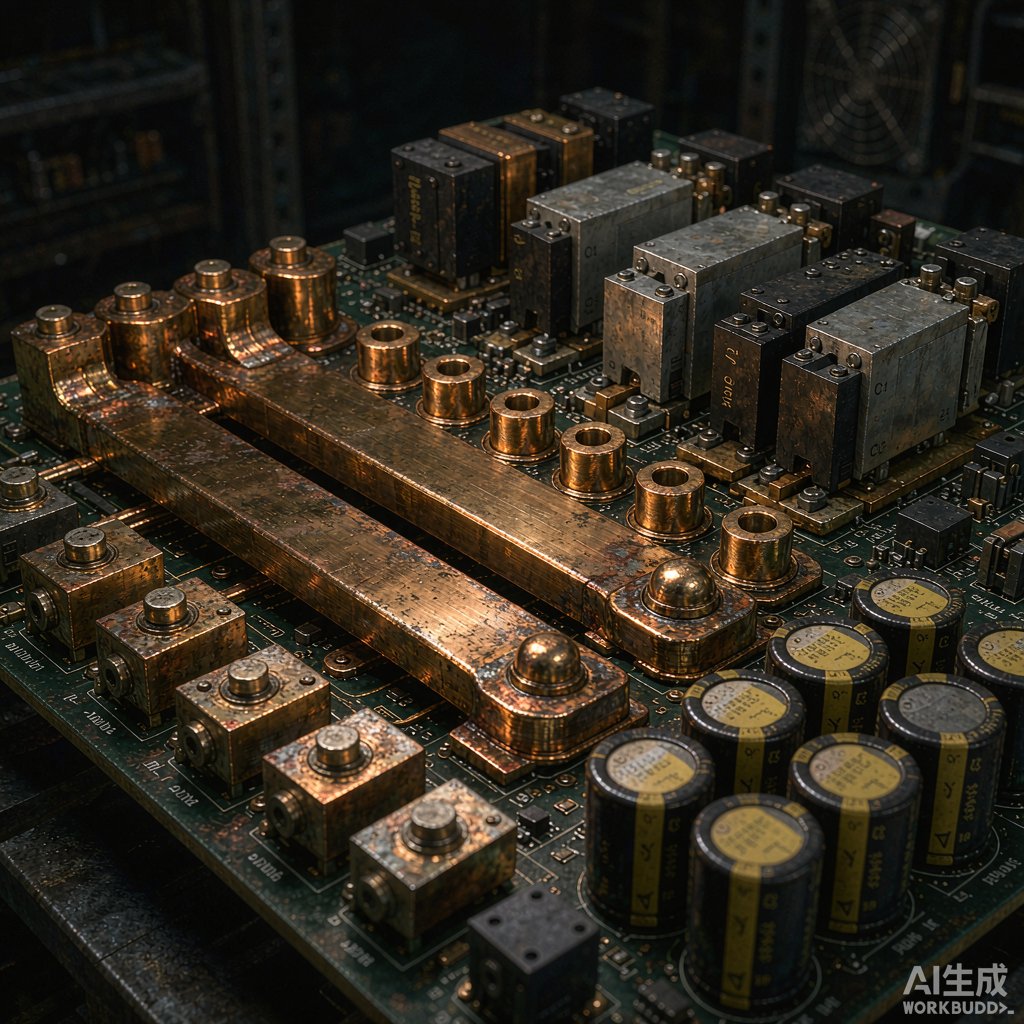
Standard PCB copper weighs 1 to 2 oz per square foot, about 35 to 70 microns thick. Power electronics – motor drives, solar inverters, onboard chargers, LED drivers – routinely ask for more. Heavy copper PCBs, with 3 to 20 oz (105 to 700 micron) layers, move substantial current on the board itself, spread heat into the laminate, and shrink or eliminate external busbars. Understanding what heavy copper can and ca
ot do keeps designs both reliable and manufacturable.
What Counts as Heavy Copper
The industry generally draws the line at 3 oz. Between 3 and 6 oz, fabrication is an extension of normal processes; beyond 10 oz, plating and etching become specialty work with wider tolerances and longer lead times. Heavy copper layers are usually built by electroplating additional copper onto a thi
er base foil inside the pattern, so final thickness varies with feature size: wide planes plate thicker than narrow traces, and design rules must account for that gradient. Expect plus or minus 20 percent thickness variation on aggressive builds unless the fabricator confirms tighter control.
Thermal Benefits Beyond Current Carrying
In-Plane Heat Spreading
A thick copper plane is an excellent lateral heat spreader. Copper conducts roughly 400 W/mK in-plane, many times better than FR-4, so a 4 oz plane under a hot component pulls heat away from the die and spreads it across the board where it can leave through convection and mounting hardware. This is the same physics behind copper heat spreaders and graphite sheets, but integrated into the board itself. For concentrated loads like a 20 W diode or an LED pad, adding a thick copper puddle layer beneath the component often lowers junction temperature more cheaply than adding a metal-core substrate.
Via Current Capacity and Stacking
Heavy copper transforms via performance too. Plating fills the barrel with 100 microns or more of copper, so a single via that would carry 2 A at standard plating can carry 8 A or more. Filled and capped vias over heavy planes also conduct heat vertically into i
er spreader layers or a backside heatsink. When several hot components share a board, a buried heavy-copper heat plane co
ected by arrays of filled vias acts like a liquid-free cold plate.
Current Capacity and IR Drop
Current capacity scales with cross-section, and heavy copper multiplies it dramatically. A 3 mm-wide external trace at 210 microns (6 oz) presents 0.63 mm2 of copper – comfortably 15 to 20 A continuous with modest rise, and far more with airflow. IR drop falls in proportion, which matters for milliohm-level paths like current shunt runs and gate-drive returns. Because thick traces also lower resistance noise and hot-spot gradients, heavy copper frequently improves measurement accuracy in power supplies, not just reliability.
Manufacturing Limits to Respect
Etching thick copper produces trapezoidal traces: the etchant undercuts, so a 210-micron trace loses proportionally more cross-section than a 35-micron one. Fabricators compensate by widening traces and enforcing minimum spacing rules that grow with thickness – 6 oz copper typically demands 0.5 mm spacing minimums and larger pad a
ular rings. Aspect ratios for vias, registration across thick layers, and solder mask over heavy features all need fabricator-specific rules. Get the stackup reviewed by the fab before finalizing; a design trivial at 2 oz can be unbuildable at 12 oz without adjustment.
When Heavy Copper Beats the Alternatives
Choose heavy copper when current paths must stay on the board, when heat sources are spread across the layout rather than concentrated at one bolt-down point, and when co
ector or busbar count needs reducing. Prefer busbars or stamped strip when currents exceed roughly 50 to 100 A per path, when the geometry is three-dimensional, or when field replacement is required. Metal-core PCBs win when heat flux is extreme and concentrated; heavy copper wins when the board must both carry and cool. Many high-power designs combine approaches: heavy copper planes for distribution and spreading, with a local metal core or cold plate under the hottest device.
Conclusion
Heavy copper PCBs push board copper from a passive conductor into an active thermal and power component. Design within etching and plating realities, use thick planes to spread heat and filled vias to move it vertically, and compare against busbars and metal-core options on a per-path basis. Done well, heavy copper consolidates functions that would otherwise demand extra parts, assemblies, and failure points.



