Why the Heat Spreader Architecture Matters
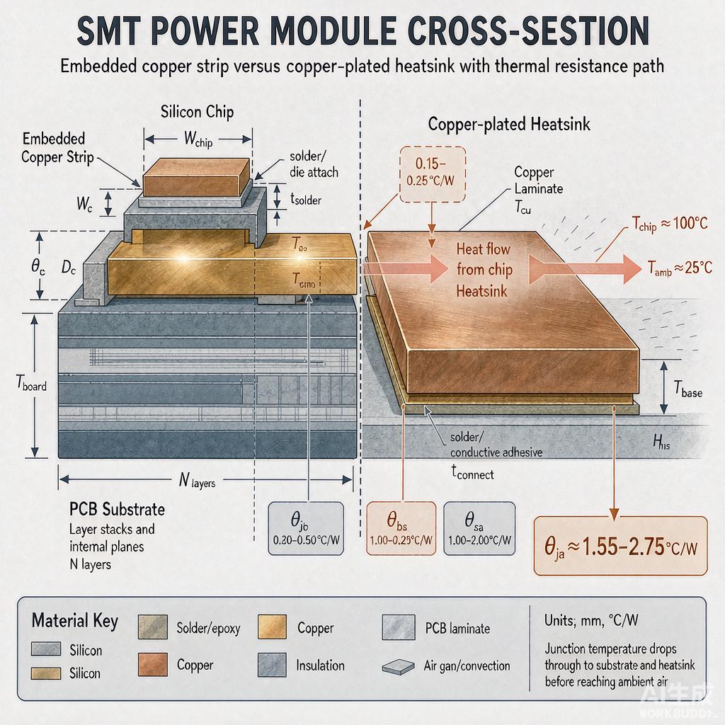
Surface-mount power modules-IGBTs, MOSFETs, GaN switches, high-current LED drivers, and DC-DC converters-dissipate 5-100 W of heat from a small package footprint. The thermal path from the silicon die to the PCB and ultimately to ambient determines junction temperature, device lifetime, and maximum operating current. Two dominant SMT thermal-management architectures compete in this space: copper strip inlay substrates and copper-plated heatsinks. Both deliver improved thermal performance over standard FR-4 PCB substrates, but they differ substantially in manufacturing process, thermal resistance, cost, and reliability. This article presents side-by-side comparison data from manufacturer datasheets and industry qualification studies.
Copper Strip Inlay Construction
Process Flow
Copper strip inlay substrates are manufactured by inserting a precision-cut copper bar into a milled or routed cavity in the i
er PCB core and bonding it under heat and pressure during lamination:
- Cavity preparation: CNC mill or laser-cut the cavity in the i
er core at the location of the SMT power device footprint. Typical cavity depth: 0.5-1.5 mm; typical inlay thickness: 0.8-1.2 mm.
- Surface preparation: Micro-etch or black oxide treatment on the cavity walls to improve bond strength.
- Strip placement: Pick-and-place the pre-cut C1100 (OFHC) or C1020 (DHP) copper strip into the cavity; alignment tolerance ±0.05 mm.
- Prepreg bonding: Stack the inlaid core with B-stage prepreg and outer copper foils, then vacuum laminate at 180-200°C and 200-300 psi for 90-120 minutes.
- Drilling and plating: Standard PCB fabrication steps; vias can be drilled through the inlay if electrical co
ection to the strip is needed (laser-drilled microvias preferred).
Final inlay thickness after lamination is 0.6-1.0 mm within the PCB thickness envelope. The copper strip becomes a continuous thermal highway from the SMT device pad to the opposite side of the PCB, dramatically reducing thermal resistance to a bottom-side heatsink.
Copper Materials and Grades
Common copper strip grades used in PCB inlay:
- C1100 (OFHC): 99.99% pure copper, 391 W/m·K thermal conductivity. Best for thermal performance, but expensive and soft.
- C1020 (DHP): 99.95% copper + 0.03% phosphorus. Thermal conductivity 350-380 W/m·K; higher mechanical strength than C1100.
- C19400 (Cu-Fe-P alloy): 99.0% Cu + 2.4% Fe + 0.1% P. Thermal conductivity 170 W/m·K; optimized for high-temperature strength and lead-free reflow survival.
For thermal performance-critical applications, specify C1100 or C1020. For designs that demand high thermal cycling reliability, C19400 offers better fatigue strength even at the cost of 50% lower thermal conductivity.
Copper-Plated Heatsink Construction
Electroplating Process
Copper-plated heatsinks are manufactured entirely as a metallization stack on the PCB surface:
- Base substrate: FR-4, high-Tg FR-4, or metal-core PCB (MCPCB) with aluminum or copper base plate.
- Copper plating: Electrolytic deposition of copper 50-200 µm thick on the device footprint, through a patterned dry-film photoresist. Acid copper sulfate bath with brightener and leveler additives.
- Surface finish: ENIG (Electroless Nickel Immersion Gold) or OSP (Organic Solderability Preservative) on top of the copper.
- Optional nickel plating: 3-10 µm electroless or electrolytic nickel layer under the gold for diffusion barrier and harder surface.
Plated heatsinks integrate directly with standard PCB SMT assembly lines. No special cavity milling or strip placement is required. The PCB is fabricated entirely through conventional processes.
Thermal-Via Arrays Combine with Plating
Plated heatsinks typically work in combination with thermal-via arrays: arrays of 0.3-0.5 mm drilled or laser-vias plated with copper, placed under the heat-generating component. Common configurations:
- Via array pitch: 1.0-1.5 mm center-to-center.
- Via diameter: 0.3 mm drilled, 0.5-0.8 mm pad diameter after plating.
- Plating thickness: 25 µm standard, up to 50 µm for enhanced thermal performance.
- Via fill: Conductive or non-conductive epoxy fill to prevent solder wicking during reflow.
The thermal-via-plus-plated-heatsink combination typically achieves 60-80% of a copper inlay’s thermal performance while remaining within standard PCB processing capabilities.
Thermal Resistance Comparison
Measurement Methodology
Thermal resistance is measured using JEDEC JESD51 family methods, particularly the JESD51-14 transient dual-interface test. A heat source is mounted on the test board, and thermal resistance from junction to ambient (θJA) or junction to case (θJC) is calculated from the cooling curve. For SMT power modules on 100×100 mm boards, typical results:
| Architecture | θJB (°C/W) | θJA on Still Air (°C/W) | θJA with 200 LFM Airflow (°C/W) |
|---|---|---|---|
| Standard FR-4, no thermal management | 45-60 | 70-90 | 45-55 |
| FR-4 + thermal vias + 50 µm Cu plating | 20-28 | 35-45 | 22-30 |
| FR-4 + dense thermal vias + 100 µm Cu plating | 14-20 | 28-35 | 16-22 |
| FR-4 with C1020 inlay (0.8 mm) + bottom heatsink | 8-12 | 20-28 | 10-15 |
| 10-15 | 25-32 | 12-18 | |
| 5-8 | 15-22 | 6-12 |
Practical Implications
For a 25 W SMT power MOSFET dissipating 25 W in a still-air application, the temperature rise with standard FR-4 would be 1750°C-well above silicon junction limit. A plated heatsink solution reduces rise to 625-1125°C, still over limits. A copper inlay solution reduces rise to 200-300°C, well within the 150°C junction limit at ambient 25°C. The thermal performance gap is decisive for high-power designs.
Thermal Cycling Reliability
IPC-9701 Thermal Cycling Qualification
Both architectures are qualified to IPC-9701 with -40°C to +125°C or 0°C to +100°C temperature excursions. Failure modes:
- Inlay substrates: Crack propagation in the resin around the inlay edges; copper-to-resin delamination at the bonding interface; fatigue of the inlay-resin interface. Typically rated for 1000-2000 cycles to first electrical failure.
- Plated heatsinks: Plated copper fatigue cracks at via necks; solder joint fatigue at the device terminations; resin cracking under heavy plating. Typically 1500-3000 cycles depending on plating thickness and via design.
Plated heatsinks generally show better thermal cycling life than inlays because the plating and vias experience more uniform strain than the inlay-resin interface. However, the inlay’s larger thermal mass reduces diurnal temperature swings, partially offsetting this advantage.
Power Cycling Reliability
Under power cycling (on/off with internal heating), inlay substrates show 2-3x longer life than plated heatsinks because the thermal gradient flows primarily through the thick copper block, reducing stress on the device-to-PCB solder joint. For an IGBT module in an automotive inverter application, inlay construction extends power cycle life from 50,000 cycles to over 150,000 cycles at ΔTj = 100°C.
Cost Structure and Lead Time
Cost Comparison
On a per-square-decimeter basis for 1.6 mm total thickness PCB:
- Standard FR-4: $0.08-0.15/dm².
- FR-4 + thermal vias + ENIG: $0.30-0.55/dm².
- FR-4 + heavy copper plating (100 µm): $0.80-1.40/dm².
- FR-4 + inlay (C1020, 0.8 mm): $2.50-4.50/dm².
- MCPCB (Al or Cu base): $0.90-2.00/dm².
The inlay command a 4-8x cost premium over standard FR-4 and 2-3x premium over plated heatsinks. For high-power designs that genuinely require the thermal performance, the premium is justified by reduced heatsink requirements, smaller PCB area, or extended lifetime.
Lead Time
Inlay substrates typically require 4-8 weeks lead time at standard PCB fabricators, compared to 2-3 weeks for heavy-copper-plated FR-4 and 3-4 weeks for MCPCB. Custom cavity milling or inlay geometry adds another 1-2 weeks for tooling setup. For prototype work, MCPCB or heavy-copper-plated FR-4 is preferred for fast iteration; inlay is reserved for production designs once the geometry is fixed.
Application Selection Matrix
- Choose copper inlay when: continuous power dissipation >30 W per device, junction-to-ambient thermal budget <20°C/W, expected lifetime >10 years in harsh thermal cycling environment.
- Choose plated heatsink when: 5-25 W power, cost-sensitive application, prototype development, moderate thermal cycling requirements.
- Choose MCPCB when: LED lighting, moderate-power industrial motor drivers, applications where 1-sided cooling is acceptable.
For most high-volume consumer electronics applications, the plated heatsink strikes the best balance; for premium industrial and automotive applications, inlay construction is preferred; for LED lighting, MCPCB remains the dominant choice due to its mature supply chain and predictable long-term cost.



