Introduction: When PCB Grounding Creates an Ante
a
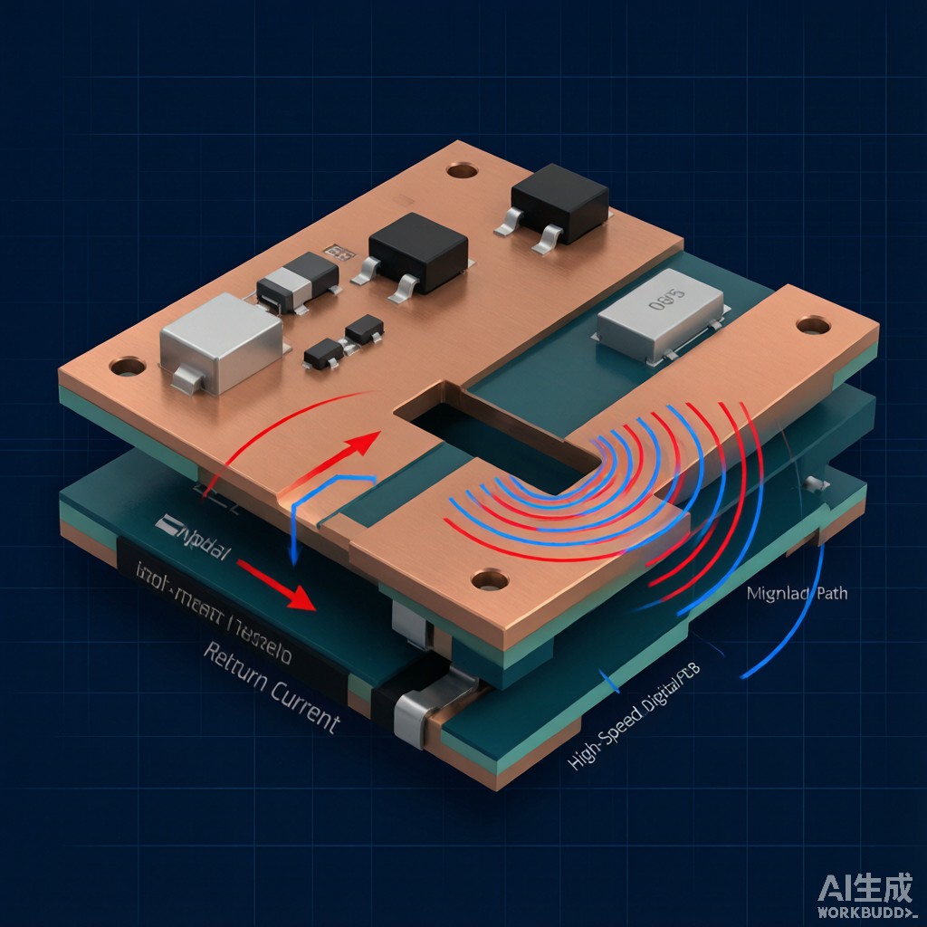
One of the most counterintuitive lessons in high-speed PCB design is that a poorly designed ground plane — intended to suppress EMI — can itself become a powerful radiator of electromagnetic interference. When a continuous ground plane is interrupted by a gap, slot, or split — whether by design (separating analog and digital grounds) or by oversight (via clusters, co
ector cutouts, routing cha
els) — the resulting discontinuity forms a slot ante
a. At frequencies where the slot length approaches half the wavelength (λ/2) or its harmonics, a seemingly benign gap in the ground plane radiates EMI with efficiency that can rival intentional ante
as.
This article examines the physics of slot ante
a radiation from ground plane discontinuities, the conditions under which return path gaps become significant EMI sources, and the engineering techniques that mitigate slot radiation in high-speed mixed-signal PCB designs.
Physics of the Slot Ante
a Effect
Babinet’s Principle and Slot Radiation
According to Babinet’s principle in electromagnetics, a slot in an infinite conducting plane is the complement of a dipole ante
a. A slot of length L cut into a ground plane radiates identically to a dipole of the same length — but with the electric and magnetic fields interchanged. A horizontal slot radiates vertically polarized waves, while a horizontal dipole radiates horizontally polarized waves.
The resonant frequency of a slot ante
a is given by:
f_resonant = c / (2L)
Where c is the speed of light (3 × 10⁸ m/s) and L is the slot length in meters. At resonance, the slot radiation resistance is approximately 485 Ω — meaning a slot ante
a can be more efficient than a half-wave dipole (73 Ω) when properly fed.
| Slot Length L (mm) | Resonant Frequency (GHz) | λ/2 at Resonance (mm) | Relevant Digital Protocols |
|---|---|---|---|
| 100 | 1.5 | 100 | DDR3, LPDDR3 |
| 50 | 3.0 | 50 | DDR4, PCIe Gen2, SATA III |
| 30 | 5.0 | 30 | USB 3.0, PCIe Gen3, DDR5 |
| 15 | 10.0 | 15 | 10 GbE, USB 3.1 Gen2 |
| 10 | 15.0 | 10 | PCIe Gen4 (16 GT/s) |
| 7.5 | 20.0 | 7.5 | PCIe Gen5 (32 GT/s), USB4 |
| 5 | 30.0 | 5 | PCIe Gen6, 5G FR2 (mmWave) |
The critical insight: as digital bus speeds increase, even small ground plane gaps become resonant at the fundamental frequency or its harmonics. A 15 mm slot in a DDR5 PCB ground plane resonates at 10 GHz — well within the harmonic content of DDR5 signals with 2–3 ns rise times (equivalent bandwidth ~5–10 GHz).
Return Path Discontinuity as the Excitation Source
A slot in the ground plane becomes a radiating ante
a only when it is excited by a time-varying current. The excitation source is invariably a return path discontinuity — a signal trace that crosses over the slot, forcing its return current to diverge from the intended path directly beneath the trace.
At low frequencies (below ~100 kHz), return current spreads broadly through the ground plane — resistance dominates, and the current takes the path of least resistance. At high frequencies (above ~1 MHz), inductance dominates — and the return current follows the path of least inductance, which is the path directly beneath the signal trace. When the trace crosses a ground plane slot, the return current must detour around the slot, creating a large current loop area and, consequently, significant differential-mode radiation.
| Condition | Return Current Path | Loop Area | Radiation Risk |
|---|---|---|---|
| Continuous ground plane | Directly beneath trace, minimal area | h × L (h = dielectric height) | Low |
| Trace crosses slot (no stitching) | Detours around slot ends | ~ slot length × detour distance | High |
| Trace crosses slot (with stitching capacitor) | Through capacitor, small detour | ~ capacitor body length × h | Moderate |
| Trace crosses slot (with guard trace) | Via stitching, minimal detour | ~ via spacing × h | Low |
A trace carrying a 100 mA, 1 GHz signal crossing a 30 mm slot without mitigation can produce radiated emissions 20–30 dB above FCC Part 15 Class B limits at 3 m — a guaranteed EMC test failure.
Common Causes of Ground Plane Slots in PCB Layout
Design-Intentional Splits (Often Problematic)
| Split Type | Rationale | Risk Level | Recommendation |
|---|---|---|---|
| Analog-digital ground split | Isolate noisy digital return currents from sensitive analog | High | Use single unified ground with careful component placement and routing segregation |
| Power plane isolation moat | Isolate switching power supply noise | Moderate | Keep moat narrow (<2 mm), use ferrite bead bridges at signal crossings |
| High-voltage isolation gap | Safety isolation (creepage/clearance per IEC 60950) | Low (necessary for safety) | Route no signals across gap; use optocouplers or digital isolators |
| Co
ector cutout |
Through-hole co
ector mounting |
Moderate | Provide stitching vias along cutout perimeter at λ/20 spacing |
Unintentional Discontinuities
Far more common than deliberate splits are unintentional ground plane gaps created during layout:
- Via anti-pad clustering: Dense BGA escape routing creates overlapping anti-pads that merge into a continuous slot through the ground plane on i
er layers. A single BGA with 0.8 mm pitch can create anti-pad chains 5–15 mm long.
- Co
ector footprint keep-out zones:
Through-hole coectors with mounting holes create fixed gaps. High-density co
ectors (HDMI, USB-C, PCIe edge co
ectors) often have metal shell grounding tabs that create discontinuous ground areas.
- Board outline cutouts and mounting holes: Mechanical features that penetrate all layers create permanent ground plane discontinuities that ca
ot be stitched.
- Routing cha
els in dense layouts:
When signal routing density forces long parallel trace groups, the collective anti-pad overlap on the adjacent ground layer can form an elongated slot.
Mitigation Techniques
1. Stitching Capacitors — The Quick Fix
The most common mitigation for a ground plane slot is a stitching capacitor — a capacitor (typically 10–100 nF, MLCC X7R, 0402 or 0603) placed across the slot at the signal crossing point. The capacitor provides a low-impedance path for the return current at high frequencies.
Effectiveness depends on the capacitor’s self-resonant frequency (SRF):
| Capacitance | Package | Typical SRF | Effective Bandwidth | Cost per 1k |
|---|---|---|---|---|
| 100 nF | 0402 | 15–25 MHz | Narrow; above SRF, ESL dominates | $0.003 |
| 10 nF | 0402 | 50–80 MHz | Moderate; works up to ~500 MHz | $0.003 |
| 1 nF | 0402 | 200–300 MHz | Good; effective up to ~2 GHz | $0.003 |
| 100 pF | 0402 | 800–1,200 MHz | Best for GHz; effective up to 5 GHz | $0.005 |
Above the SRF, the capacitor behaves inductively (ESL typically 0.3–0.8 nH for 0402), and its impedance rises with frequency — rendering it ineffective as a return path. For signals with harmonic content above 1 GHz, a single stitching capacitor is insufficient; multiple capacitors in parallel (e.g., 1 nF + 100 pF) or a direct copper bridge (guard trace) is required.
2. Guard Traces with Via Stitching
A guard trace is a narrow copper trace placed on the signal layer, ru
ing alongside the signal trace and co
ected to the ground plane on both sides of the slot through closely-spaced stitching vias. Unlike a stitching capacitor, a guard trace provides a continuous low-impedance path with no SRF limitation.
Design rules for effective guard traces:
- Via spacing (s): s ≤ λ/20 at the highest frequency of concern. For 5 GHz, λ/20 = 3 mm. For 10 GHz, λ/20 = 1.5 mm.
- Guard trace width: Minimum 0.2 mm; wider is better but consumes routing space.
- Distance from signal trace (d): d ≤ 3 × h (h = dielectric height to ground plane). For a 4-layer board with 0.2 mm prepreg, d ≤ 0.6 mm.
- Via diameter: 0.2–0.3 mm finished hole; smaller vias have lower parasitic inductance.
3. Ground Plane Re-unification
The most effective — and most overlooked — solution is to avoid creating the slot in the first place. For mixed-signal designs, the modern consensus (Henry Ott, “Electromagnetic Compatibility Engineering”) recommends a single, continuous ground plane for all circuitry, including analog, digital, and RF sections. Partitioning is achieved through component placement (digital ICs in one zone, analog in another, with a buffer zone between) rather than through ground plane splitting.
The key insight: a 0.5 mm wide gap in the ground plane provides essentially zero isolation at frequencies above a few MHz due to capacitive coupling across the gap. The gap creates an EMI radiator without achieving its intended isolation purpose — a lose-lose design choice.
4. Reference Plane Jump Vias
When a signal must change reference planes (e.g., from layer 3 ground to layer 4 ground on a multi-layer board), a reference plane jump via must be placed within 1 mm of the signal via. This via co
ects the two ground planes at the exact point where the return current needs to transfer, preventing the return current from finding a distant return path that creates a large loop area.
Simulation and Measurement
Pre-Layout Simulation
3D full-wave electromagnetic simulation tools (Ansys HFSS, CST Microwave Studio, Keysight EMPro) can predict slot radiation before PCB fabrication. A 2.5D solver (such as in Keysight ADS or Cadence Sigrity) is typically sufficient for initial slot screening, providing S-parameter and far-field radiation predictions in minutes rather than hours.
Key simulation outputs to check:
- Maximum E-field at 3 m (dBμV/m) vs frequency — compare against FCC/CISPR limits
- Return loss (S11) at slot crossing — dips indicate resonance and efficient radiation
- Near-field H-field distribution — hotspots indicate return current concentrations around slot edges
Production Validation
Near-field H-field probes (1–10 mm loop diameter, 30 MHz–6 GHz bandwidth) co
ected to a spectrum analyzer provide rapid production-line validation of slot radiation. The probe is sca
ed along suspected slot locations while the board operates; a 6–10 dB increase in near-field level when the probe crosses the slot confirms radiation.
Design Checklist for Slot-Free Ground Planes
- Use a single continuous ground plane for all circuit sections; partition by placement, not by plane splits.
- Review all layers for anti-pad chains longer than 5 mm — these form unintentional slots.
- Place stitching vias around co
ector cutouts at λ/20 spacing (≤3 mm for 5 GHz designs).
- Where signals must cross unavoidable gaps, use guard traces with via stitching (not stitching capacitors, which fail above their SRF).
- For BGA escape routing, stagger anti-pad positions on adjacent layers to prevent chain formation.
- Run post-route DRC checks for ground plane copper continuity, focusing on areas beneath high-speed signal routes.
- During EMC pre-compliance testing, scan the PCB with a near-field H-field probe along all suspected slot locations.
Conclusion
The ground plane slot ante
a effect transforms a seemingly minor PCB layout oversight into a primary EMI failure mode in high-speed designs. As digital edge rates push into the sub-nanosecond regime, even small discontinuities — BGA anti-pad chains, co
ector cutouts, and routing cha
els — become efficient slot radiators at the fundamental and harmonic frequencies of modern digital buses. By understanding the physics of slot radiation, implementing guard traces with via stitching at critical crossing points, and adopting a single-ground-plane partitioning strategy for mixed-signal designs, PCB engineers can eliminate a class of EMI failures that are notoriously difficult to debug and expensive to fix in production.



