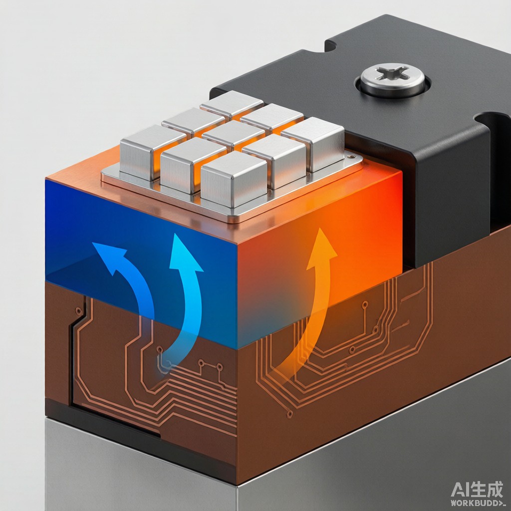
High-power LED modules operating at 50-300W present a fundamental thermal management challenge: the electrically insulating dielectric layer in conventional metal-core PCBs (MCPCBs) creates a significant thermal barrier, typically adding 0.5-2.0 K·cm²/W of thermal resistance. Thermoelectric separation copper-based PCBs address this limitation by physically separating electrical traces from thermal conduction paths, enabling direct copper-to-copper heat spreading without intermediate dielectric. This article examines the design principles, manufacturing methods, and thermal performance advantages of thermoelectric separation architecture for high-power LED and power electronics applications.
The Thermal Barrier Problem in Conventional MCPCBs
Dielectric Thermal Resistance
Standard aluminum MCPCBs use a thermally conductive dielectric layer (typically epoxy-based with ceramic filler, 75-150 μm thick) to electrically isolate copper traces from the aluminum base plate. Even with “high thermal conductivity” dielectrics claiming 2-3 W/m·K, the layer introduces substantial thermal resistance:
Rθ,dielectric = t / (k × A)
For a 1 mm² LED chip on a dielectric with t = 100 μm and k = 2.5 W/m·K: Rθ = 0.0001 / (2.5 × 0.000001) = 40 K/W. For a 10W LED dissipating 7W as heat, this creates a 280°C temperature rise—clearly unacceptable.
Copper-Based PCB Alternatives
| PCB Type | Thermal Resistance (K·cm²/W) | Max Power Density | Cost Factor |
|---|---|---|---|
| Standard FR-4 | 15-25 | <0.5 W/cm² | 1.0× |
| Aluminum MCPCB | 0.5-2.0 | 5-15 W/cm² | 2.5× |
| Copper MCPCB | 0.3-1.2 | 10-25 W/cm² | 4.0× |
| Thermoelectric separation Cu PCB | 0.03-0.08 | 50-150 W/cm² | 6-8× |
| Direct bonded copper (DBC) | 0.01-0.03 | 100-300 W/cm² | 10-15× |
Thermoelectric Separation Architecture
Design Principle
Thermoelectric separation copper PCBs achieve their exceptional thermal performance through a simple but elegant structural i
ovation: the LED mounting pad (thermal pad) is fabricated as a direct extension of the copper base plate, with electrical isolation provided only where needed for circuit routing. The architecture comprises three functional zones:
- Thermal conduction zone: The central LED mounting area maintains direct metallic continuity with the copper substrate, providing thermal resistance equivalent to bulk copper (k = 398 W/m·K).
- Electrical isolation zone:
A narrow ring (typically 0.3-0.8 mm wide) of high-temperature thermally conductive material (often Al₂O₃-filled epoxy or direct ceramic insulator) separates the thermal pad from electrical traces.
- Circuit routing zone: Standard copper traces (35-105 μm thick) on a thin dielectric layer handle electrical interco
ection between LED pads and external circuitry.
Cross-Sectional Structure
A typical thermoelectric separation copper PCB for a COB (Chip-on-Board) LED module has the following layer stack:
- Top copper circuit layer: 35-70 μm electro-deposited copper, patterned for LED anode/cathode traces and wire bonding pads.
- Thin dielectric layer: 60-100 μm polyimide or high-Tg epoxy, restricted to circuit routing areas.
- Copper base plate: 1.0-3.0 mm thick C11000 or C19400 copper, serving as both mechanical substrate and primary heat spreader.
- Surface finish: Electroless nickel/immersion gold (ENIG) on circuit traces; bare copper or silver plating on thermal pads for direct die attachment.
Thermal Performance Analysis
Heat Conduction Path
The thermal resistance network from LED junction to ambient simplifies dramatically with thermoelectric separation:
Rθ,j-a = Rθ,j-c + Rθ,c-s + Rθ,s-h + Rθ,h-a
Where Rθ,j-c (junction-to-case, determined by LED package) and Rθ,h-a (heatsink-to-ambient, determined by cooling system) are external to the PCB. The critical PCB contribution is Rθ,c-s (case-to-substrate), which for thermoelectric separation equals the thermal resistance of the copper base plate thickness:
Rθ,c-s = t_cu / (k_cu × A) = 0.001 / (398 × 0.01) = 0.00025 K/W for a 1mm thick copper plate under a 10×10 mm LED array
This is negligible compared to conventional MCPCB dielectric resistance (0.5-2.0 K·cm²/W = 0.05-0.20 K/W for the same area).
Practical Temperature Reduction
For a 100W COB LED (75W heat load) on a 20×20 mm die:
| PCB Architecture | Rθ,c-s (K/W) | ΔT at 75W (°C) | Tjunction at 25°C ambient (°C) |
|---|---|---|---|
| Aluminum MCPCB (100μm dielectric, k=2.5) | 0.50 | 37.5 | 112.5 (with Rθ,j-c=1.0) |
| Copper MCPCB (100μm dielectric, k=3.0) | 0.42 | 31.3 | 106.3 |
| Thermoelectric separation Cu PCB | 0.04 | 3.0 | 78.0 |
| Direct Bonded Copper (DBC) | 0.02 | 1.5 | 76.5 |
The 30°C+ temperature reduction from thermoelectric separation translates directly to extended LED lifetime (L70 lumen maintenance hours approximately double for every 10°C junction temperature reduction) and enables higher drive currents for increased luminous output.
Manufacturing Methods
Etch-Back Process
The most common manufacturing approach for thermoelectric separation copper PCBs:
- Start with copper-clad laminate (CCL) on copper base plate.
- Pattern the circuit layer using standard photolithography and etching.
- Remove dielectric material from thermal pad areas using controlled depth routing or laser ablation, exposing the copper base plate.
- Plate the exposed thermal pad with silver or nickel for corrosion resistance and solderability.
- Apply solder mask, leaving thermal pads and bonding pads exposed.
Cavity Milling with Insert Process
For high-volume production, a more precise approach mills cavities into the copper base plate where thermal pads will locate, then inserts pre-formed ceramic isolation rings:
- CNC milling creates ±25 μm dimensional accuracy on cavity depth and diameter.
- Alumina (Al₂O₃, k = 25-35 W/m·K) or aluminum nitride (AlN, k = 170-230 W/m·K) ceramic rings provide electrical isolation with minimal thermal penalty.
- The ceramic ring is brazed or adhesive-bonded into the cavity, then the top circuit layer is laminated and patterned.
Design Guidelines and Best Practices
Thermal Pad Sizing
The thermal pad should be sized according to the LED chip dimensions with a 0.5-1.0 mm oversize margin for manufacturing tolerance. For multi-chip arrays, individual thermal pads for each chip outperform a single large pad because they reduce lateral spreading resistance in the copper base. The 45-degree heat spreading rule applies: effective thermal conduction area expands at approximately 45° through the copper base plate thickness.
Isolation Ring Design
The electrical isolation ring width must balance two competing requirements:
- Creepage and clearance: For 48V LED systems, IEC 60598-1 requires minimum 1.5 mm creepage distance. At 200V (typical of high-voltage LED arrays), 3.0 mm is required.
- Thermal performance: Wider isolation rings increase the area of dielectric material, slightly degrading thermal performance. A 0.5 mm ring adds approximately 0.02 K/W for a 10×10 mm pad—negligible in most applications.
Solder Mask and Surface Finish
White solder mask (reflectivity >85% at 450 nm) over non-thermal areas maximizes light extraction efficiency for LED applications. The thermal pad should remain solder-mask-free and receive either immersion silver (optimal for die attach solder) or electroless nickel/immersion silver (ENIS) for wire bonding compatibility.
Reliability Considerations
Thermal Cycling Performance
The primary reliability concern is CTE mismatch between the copper base plate (17 ppm/°C), dielectric layer (15-50 ppm/°C depending on material), and LED package (typically ceramic at 6-7 ppm/°C or silicon at 2.6 ppm/°C). Thermoelectric separation actually improves reliability by minimizing the dielectric area under thermal stress:
- Standard MCPCB: Large dielectric area experiences shear stress from CTE mismatch across the full LED footprint.
- Thermoelectric separation: Dielectric restricted to narrow ring; thermal pad has no CTE mismatch because LED die attaches directly to copper.
IPC-9701 thermal cycling test data shows thermoelectric separation copper PCBs surviving 2,000 cycles (-40°C to +125°C) with less than 10% increase in thermal resistance, compared to 500-800 cycles for standard aluminum MCPCBs before dielectric delamination.
Conclusion
Thermoelectric separation copper-based PCBs represent a significant thermal performance advancement for high-power LED and power electronics applications. By eliminating the dielectric thermal barrier at the critical heat conduction path, this architecture achieves thermal resistance an order of magnitude lower than conventional MCPCBs while maintaining electrical safety isolation. For applications where junction temperature directly impacts product lifetime, reliability, and performance—such as automotive headlights, stadium lighting, and high-density power converters—thermoelectric separation copper PCBs deliver compelling engineering value despite their higher manufacturing cost.



