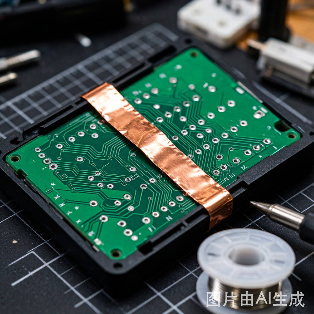
Introduction: The Gap Between Design and Production Shielding
In mass production, EMI shielding for SMT assemblies is typically implemented with precision-stamped metal cans, conductive gaskets, and electroplated housings — all designed, tooled, and validated months before the first production unit rolls off the line. But during the critical phases of product development — prototype bring-up, pre-production validation, and field failure analysis — engineers face a different challenge: how to implement effective EMI shielding quickly, reversibly, and without the six-week lead time of a custom shielding can tool.
Copper foil tape is the engineer’s answer to this challenge. A roll of conductive copper tape with pressure-sensitive adhesive costs $10–30, ships overnight, and can be cut and applied in minutes to create effective local EMI shields, ground planes, and cable wraps. This article provides a practical engineering guide to copper foil tape EMI shielding for SMT PCB rework and prototype development, covering tape selection, conductive adhesive technology, grounding best practices, and shielding effectiveness validation.
Copper Foil Tape Types and Selection
Tape Construction and Specifications
| Type | Copper Thickness | Adhesive | Conductivity | Best Application |
|---|---|---|---|---|
| Standard copper foil | 25–35 μm (1–1.4 mil) | Non-conductive acrylic | Copper only | Ground planes, non-critical shields |
| Conductive-adhesive copper foil | 25–50 μm | Conductive acrylic (Ni/Cu particles) | <0.05 Ω/sq through adhesive | EMI seams, overlapping joints |
| Double-sided conductive copper foil | 25–35 μm | Conductive on both sides | Bond + face conductive | Cable wraps, complex 3D shields |
| Embossed / dead-soft copper | 50–100 μm | Non-conductive or conductive | Copper only | Conformal shields over tall components |
| Copper foil with liner | 25–50 μm | Either type | Varies | Precision die-cut patterns |
For SMT PCB rework and prototyping, conductive-adhesive copper foil tape is the most versatile choice. The conductive adhesive (loaded with nickel-plated copper or pure silver particles at 30–40% volume fraction) provides electrical continuity across overlapping seams and between the tape and PCB ground plane, eliminating the need for soldering every joint. Standard non-conductive adhesive tape is suitable for applications where the copper face itself makes direct metal-to-metal contact with a grounded surface.
Key Selection Parameters
- Thickness: 25 μm tape is flexible and conforms to curved surfaces but provides lower shielding effectiveness at low frequencies (<100 MHz). 50 μm tape offers better low-frequency magnetic shielding but is stiffer and harder to apply around tight corners.
- Adhesive thickness: Thicker adhesive (25–50 μm) fills surface irregularities and improves contact on rough or oxidized surfaces. Thi
er adhesive (10–15 μm) provides higher peel strength on smooth surfaces.
- Temperature rating: Standard acrylic adhesive is rated to 80–100°C. For reflow-adjacent applications, silicone-based conductive adhesive rated to 150–180°C is required.
Shielding Effectiveness Fundamentals
Mechanism and Frequency Dependence
Copper foil tape provides EMI shielding through two mechanisms:
- Reflection: At high frequencies (>10 MHz), the dominant mechanism is reflection from the conductive surface. Copper’s high conductivity (σ = 5.8 × 10⁷ S/m) provides surface impedance Z_s = √(πfμ/σ), which is very low, causing most incident electromagnetic energy to reflect.
- Absorption: At low frequencies (<1 MHz), magnetic fields penetrate the conductor and are attenuated by eddy currents induced in the copper. Absorption increases with conductor thickness and frequency.
The skin depth (δ) — the distance at which field amplitude decays to 1/e — determines the minimum effective thickness:
δ = √(2 / (ωμσ)) = 66 / √f (mm) for copper, f in Hz
| Frequency | Skin Depth in Copper | 25 μm Tape Attenuation | 50 μm Tape Attenuation |
|---|---|---|---|
| 100 kHz | 0.21 mm | 10–15 dB | 20–25 dB |
| 1 MHz | 0.066 mm | 25–35 dB | 45–55 dB |
| 10 MHz | 0.021 mm | 50–60 dB | 70–80 dB |
| 100 MHz | 0.0066 mm | 70–80 dB | 90–100 dB |
| 1 GHz | 0.0021 mm | 90–100 dB | >100 dB |
At frequencies above 10 MHz, even 25 μm copper foil tape provides >50 dB of shielding — sufficient for most consumer electronics and industrial applications. At 100 kHz–1 MHz (switching power supply fundamental frequencies), 50 μm tape or multi-layer application is recommended to achieve >30 dB attenuation.
Application Techniques for SMT PCB Rework
Local Shield Patches for Noise Source Containment
During prototype debug, radiated EMI failures often trace to a single noisy component: a switching regulator, crystal oscillator, or motor driver IC. Rather than redesigning the PCB, a local copper foil tape shield can be applied over the offending component:
- Ground frame: Apply a perimeter strip of conductive-adhesive copper tape around the noise source, pressing firmly onto exposed ground vias or ground plane areas on the PCB surface. The frame should be 3–5 mm wide and form a closed loop.
- Top cover: Cut a piece of copper tape slightly larger than the shielded area. Apply it over the component, overlapping the ground frame by 2–3 mm on all sides. The conductive adhesive ensures electrical contact between the cover and the frame.
- Via stitching: For high-frequency shielding (>500 MHz), stitch the ground frame to the internal ground plane with 0.3–0.5 mm diameter wire soldered to nearby ground vias at 10–15 mm spacing. This reduces ground inductance and improves shielding by 10–20 dB.
Cable and Co
ector Shielding
Unshielded cables leaving a PCB (USB, HDMI, power) are common EMI emission paths. Copper foil tape provides temporary cable shielding:
- Wrap method: Spiral-wrap 25 μm copper tape around the cable with 50% overlap. Terminate the shield at the PCB end by pressing the tape onto a grounded co
ector shell or ground plane area.
- Pigtail grounding: At the PCB end, fold back 10 mm of tape to create a “pigtail” and solder it to a ground via or mounting hole. Keep pigtail length <20 mm to minimize inductance.
- 360° termination: For best performance, wrap the cable shield 360° around the co
ector body and secure with conductive adhesive or a copper wire “hose clamp” soldered to ground.
Ground Plane Augmentation
In prototypes with insufficient ground plane area (common in two-layer quick-turn PCBs), copper foil tape can augment the ground plane:
- Apply strips on the non-component side of the PCB, overlapping with ground vias
- Create “ground bridges” across slots or splits in the plane
- Add local ground “islands” beneath high-speed signal traces to provide return paths
Each strip should be electrically co
ected to the main ground plane at multiple points (every 20–30 mm) through vias or component ground pins to avoid creating ground loops.
Grounding Best Practices
The Critical Role of Low-Impedance Grounding
A shield without a low-impedance ground co
ection is not a shield — it is an ante
a. The shielding effectiveness of any copper foil tape application is limited by the impedance of the path from the shield to the system ground. Best practices include:
- Shortest path: Ground co
ection length should be 100 MHz applications, <30 mm for 10–100 MHz
- Multiple co
ections:
Use 3–5 ground coections distributed around the shield perimeter rather than a single point
- Wide co
ections:
A 5 mm wide tape strip has lower inductance than a 0.5 mm wire. Use tape-to-plane contact areas of >50 mm² where possible - Clean surfaces: Remove solder mask, oxidation, and conformal coating from ground contact areas using a fiberglass scratch brush or solvent wipe
Measurement and Validation
Near-Field Probe Verification
During prototype debug, a near-field H-field probe (loop ante
a, 1–3 cm diameter) co
ected to a spectrum analyzer provides rapid feedback on shielding effectiveness:
- Measure magnetic field strength 1 cm above the unshielded noise source at the offending frequency
- Apply the copper foil tape shield
- Re-measure at the same location
- Target: >20 dB reduction for local noise containment, >30 dB for regulatory compliance margin
Transfer Impedance Testing
For cable shielding validation, transfer impedance (Z_t) measures how much voltage is induced on the i
er conductor by a current flowing on the shield. Lower Z_t indicates better shielding. A copper foil tape shield with 360° termination typically achieves Z_t <10 mΩ/m at 100 MHz — comparable to commercial braided shields.
Limitations and When to Transition to Production Shielding
| Factor | Copper Foil Tape (Prototype) | Stamped Metal Can (Production) |
|---|---|---|
| Shielding effectiveness | 30–60 dB (application-dependent) | 60–100+ dB |
| Durability | Moderate (adhesive degrades over time) | Excellent (soldered or snapped) |
| Thermal management | Poor (no thermal vias, limited contact) | Good (designed thermal paths) |
| Repeatability | Low (hand-applied variation) | High (automated assembly) |
| Unit cost (material only) | $0.10–0.50 | $0.15–0.75 |
| Tooling cost | $0 | $2,000–15,000 |
| Lead time | Same day | 4–8 weeks |
Copper foil tape is a bridge technology, not a destination. Once prototype validation confirms that shielding resolves the EMI issue, the design should transition to a production-grade solution: a stamped nickel-silver or copper EMI can, a conductive gasket, or a metallized plastic housing. The tape prototype provides proof-of-concept and identifies the minimum shielding requirements (frequency range, attenuation level, grounding points) that guide the production shielding design.
Conclusion
Copper foil tape is an indispensable tool in the SMT engineer’s EMI troubleshooting kit. It provides 30–60 dB of shielding effectiveness across 100 kHz–1 GHz, requires zero tooling investment, and can be applied in minutes during a debug session. Success depends on three principles: (1) select conductive-adhesive tape for seam continuity, (2) ground the shield with multiple short, wide co
ections to the PCB ground plane, and (3) validate with near-field probes before and after application. While copper foil tape ca
ot replace production-grade shielding cans for cost, durability, and repeatability, it dramatically accelerates prototype development by enabling rapid EMI hypothesis testing without the 4–8 week lead time of custom shielding tooling. For every SMT engineer debugging a radiated emissions failure, a roll of copper foil tape should be as standard on the bench as a soldering iron.



